Siemens M1327A3, part 1
Hullo, it’s been a REAL while since the last post. Sorry, that’s how it is.
Today I’ll be writing down some thoughts on a Siemens M1327, specifically revision A3. I thought, as I have multiple samples of this device, I’d try my hand at reverse engineering it. The chip went through multiple revisions; I have seen A2 and A3 and would love to see A1. Moreover, this design seems to come after M127 which implements “similar” functionality.
All images are sourced from here.
There are two obvious memory arrays on the device. The top one is 17 columns by 16 rows, the bottom one is 14 columns by 16 rows.
Device basics
This is a depletion-mode NMOS device using polysilicon gates. Unlike CMOS, it only has N-channel transistors (duh) – with a basic building block like this:
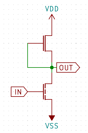
Which translates to this (least obscured) layout on the die:

The input is a poly wire going in from the left, creating a small N-ch transistor connected to a much larger one on top. The output is again a poly wire, notably as a continuation of the pull-up NMOS transistor gate.
In NMOS circuits that aren’t built from standard cells, it is paramount to be able to distinguish between transistors and everything else e.g. polysilicon wires crossing a diffusion.
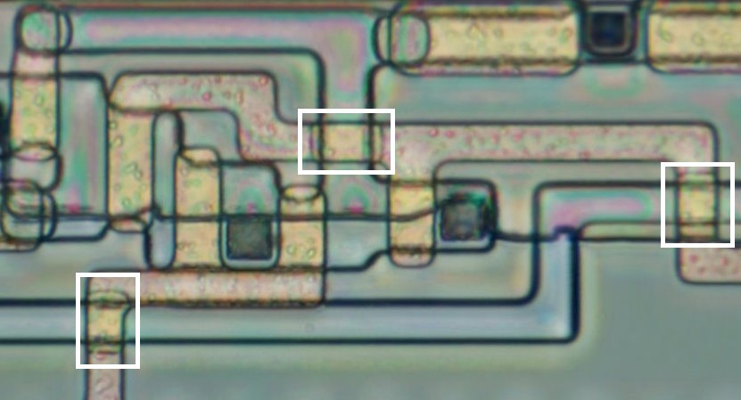
Here, we have poly wires (kinda reddish gray?) crossing a diffusion (here normally cool gray) without forming a transistor. Note the small lines on the sides; note the absence of the same on unmarked crossings.
A worked example
Let’s try reverse engineering this gate:
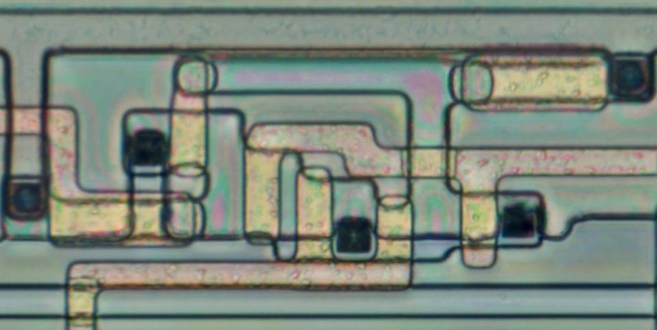
Immediately, two pull-up transistors are present, as well as several normal NMOS devices. Black rectanges are contact points from the metal layer to the diffusion layer. Here is a tentative markup of what’s going on:
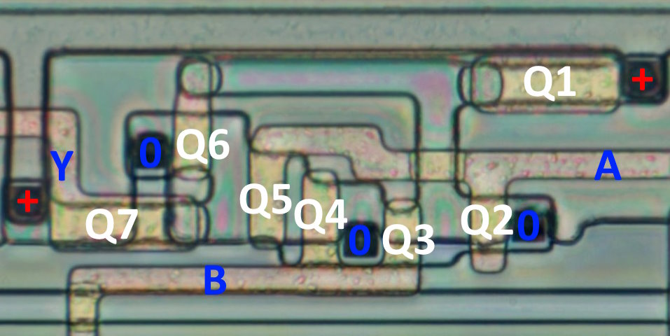
Putting this carefully into KiCad:
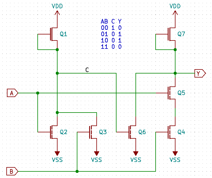
…and if I didn’t make any stupid mistakes (happens!) – this appears to be a XOR gate.
More to follow. Until then!
/DJ
UPDATE: As it was pointed out, the load transistors should be depletion-mode (solid line instead of dashed).
UPDATE 2: Part 2 has arrived.