Siemens M1327A3, part 3: The T flip-flop
Ahoy sailor, today I shall continue the exploits against Siemens M1327A3. In this post, I will look at this smol piece of circuitry, which is repeated in several places:
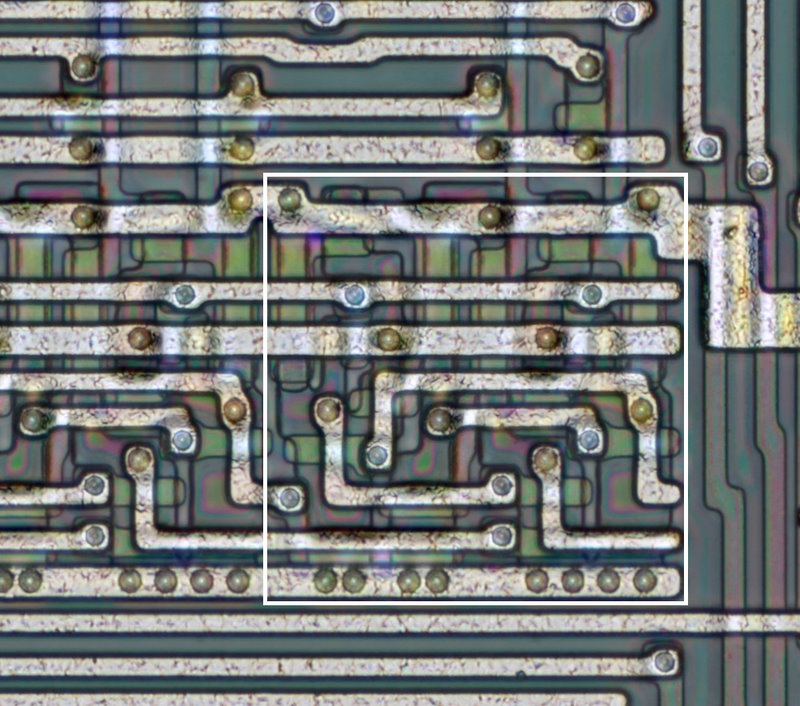
Notably, all instances are grouped and connected together one after another, plus a few common lines.
Like before, I marked up all the transistors in this block:
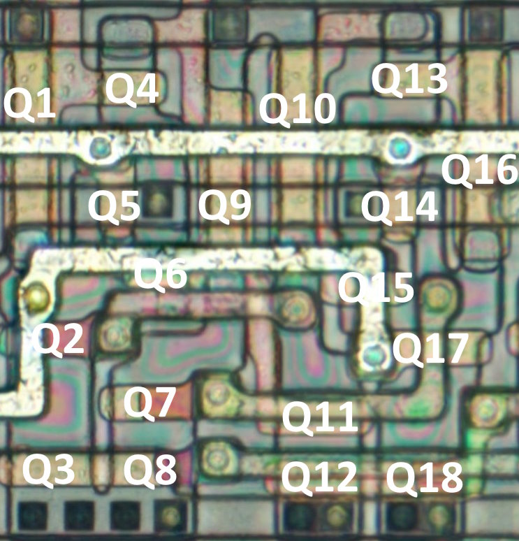
After carefully redrawing this in KiCad, I got this interesting schematic:
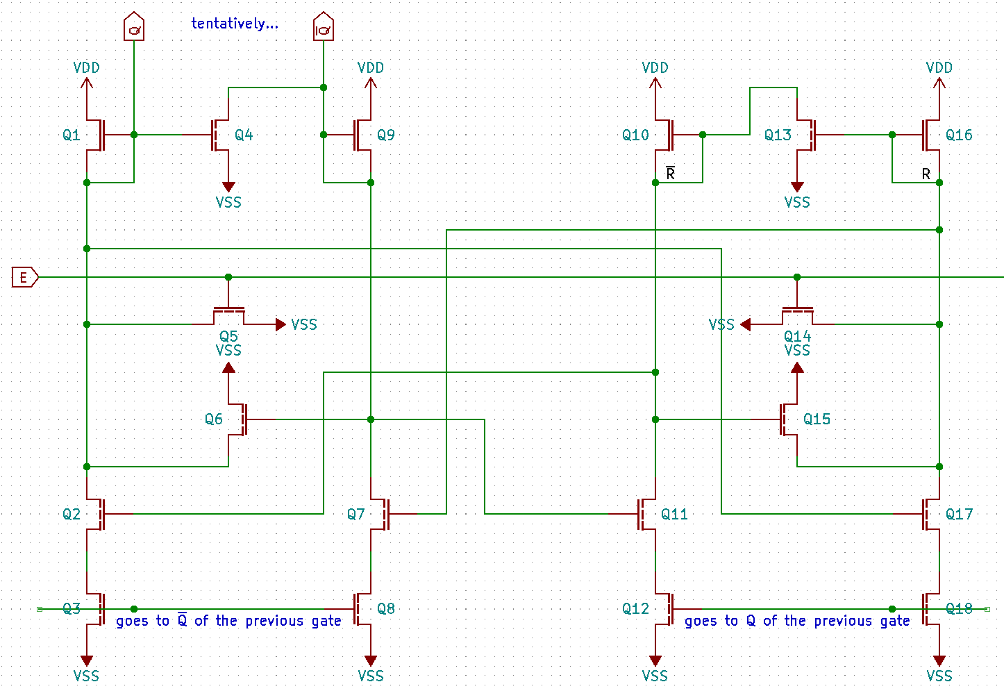
Looks like we have here two instances of the same, cross-coupled. This is probably some sort of a flip-flop circuit, the question is now what kind of a flip-flop are you? What are you going to do with your signals?
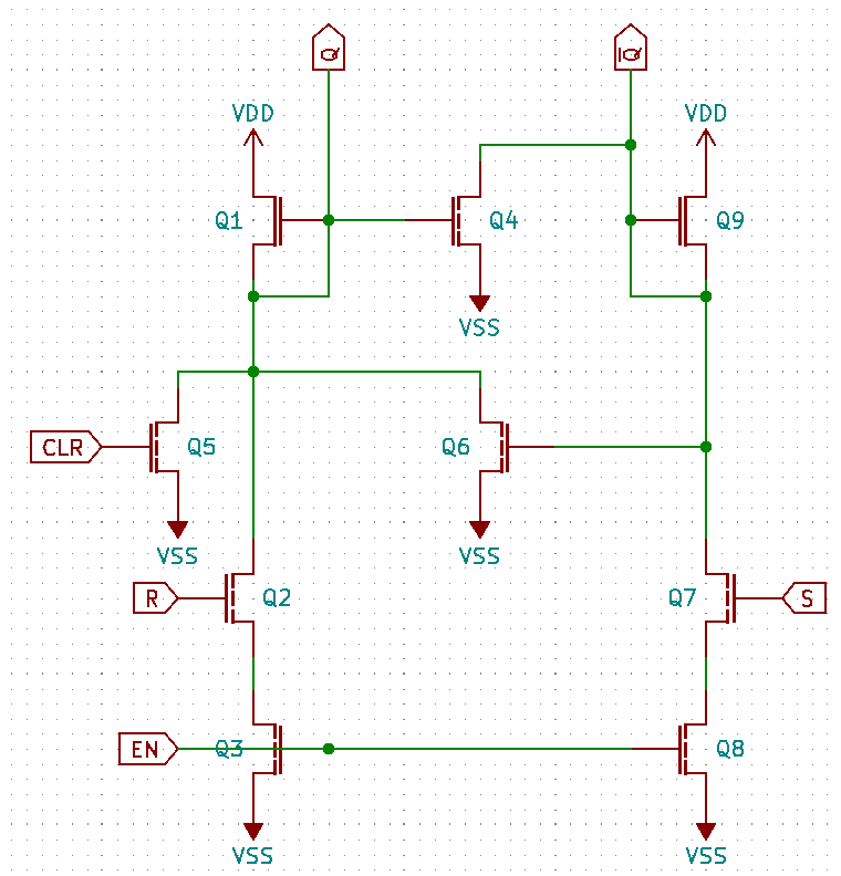
Redrawing one half of the circuit, I get more clarity as to what’s up.
Analysis
NOTE: Initially I attempted to analyse the whole thing. This led to mistakes and a general mess, so I deleted it and started anew. Sorry you’ll have to miss that.
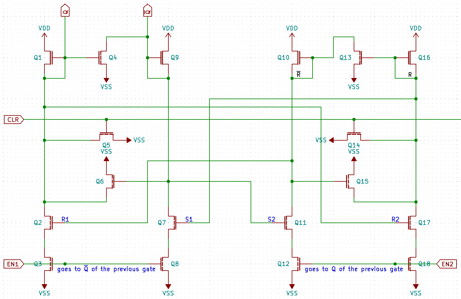
Assume the Q output is at VDD; this means Q5, and Q6 are not conducting, and both Q2 and Q3 can’t be conducting at the same time. For now, assume EN is at VSS so Q3 and Q8 don’t conduct. But Q4 does, and it pulls !Q to VSS. The circuit stays in this state even if R or S change.
OK, now I set EN to VDD; Q3 and Q8 conduct now. Assuming R and S are at VSS, nothing changes.
Now if R goes to VDD and Q2 starts conducting, Q is pulled to VSS and Q4 stops conducting. As Q7 is not conducting now (S is at VSS), !Q goes up to VDD. This turns Q6 on, and it locks the new state in place. Now even if R goes to VSS, it does not change. Similar thinking applies to the S input.
I see this as a RS-type flip-flop with enable input.
Now when CLR goes to VDD, it acts in the same way as both R and EN together, resetting Q to L. This adds a clear input.
As I know what this does in full, I can now package this into its own sub-component.
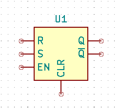
Relabelling some of the wires in the overall schematic:
And with wires labelled, it is easy to redraw it with my new symbol:
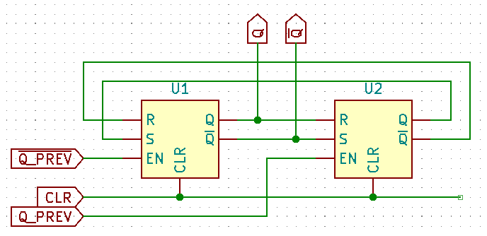
Now it’s clear what is going on! Depending on the state of the previous block, one of the two flip-flops is enabled. If U1 is enabled, it assumes the state of U2: Q goes to S, !Q goes to R. If U2 is enabled, it assumes the inverse state of U1: Q goes to R and !Q goes to S.
Imagining these blocks being chained, each next block changes its state twice as slowly as the previous one. It’s a frequency divider building block, a T flip-flop! Have several of them chained, provide a clock input and an inverse of it, and you get a divider/counter. Marking up the signals for future reference:
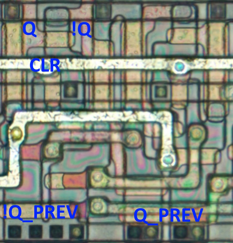
Worthy of note: the chip in question has 3 such divider/counter blocks. I will have a look at them next time. Until then!
XOXO, /DJ