Siemens M1327A3, part 7: Clock input
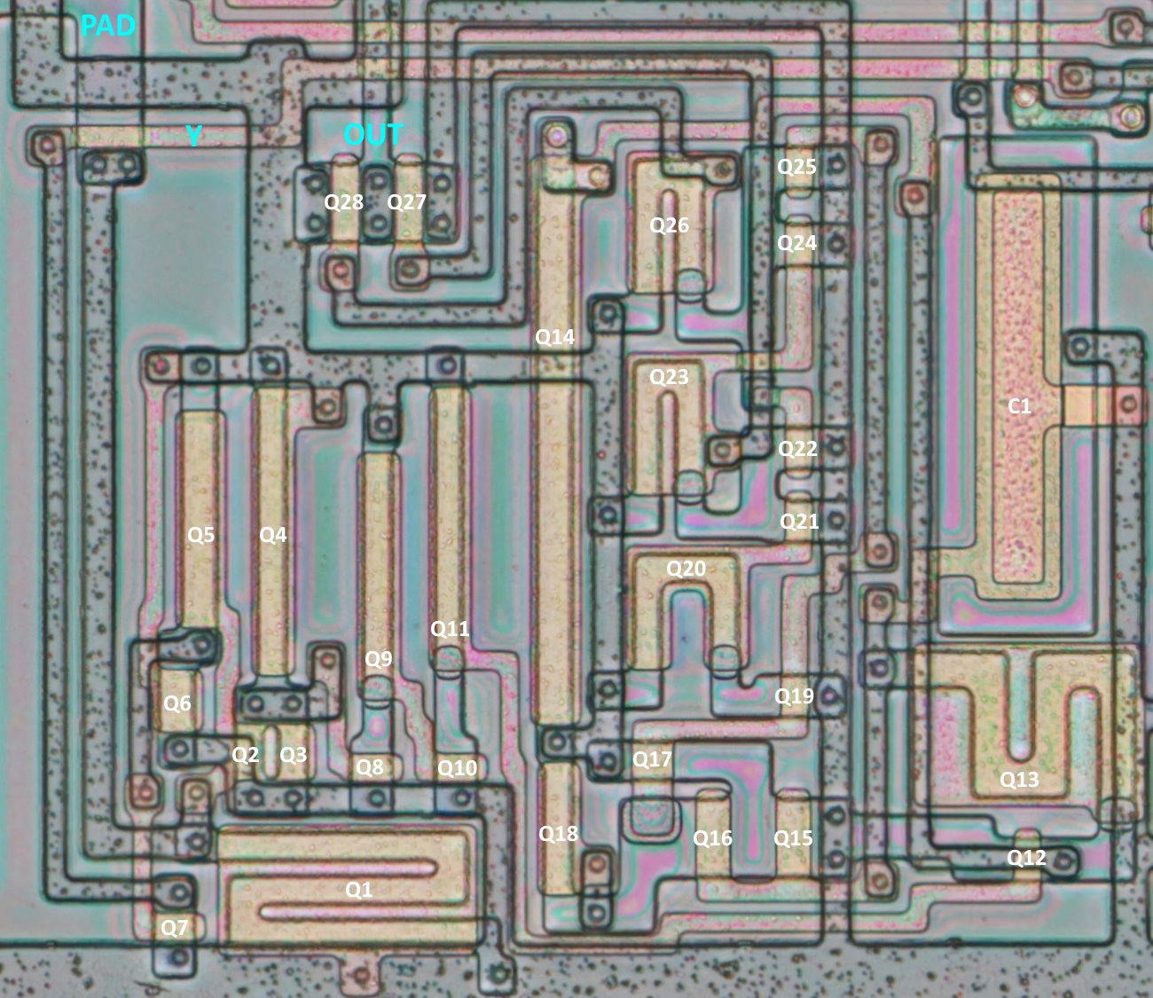
Hola! I shall continue the reverse engineering exploits against Siemens M1327A3 today. This time I will be looking at the clock input circuitry. Here is the (rotated) overview with components and signals marked up:

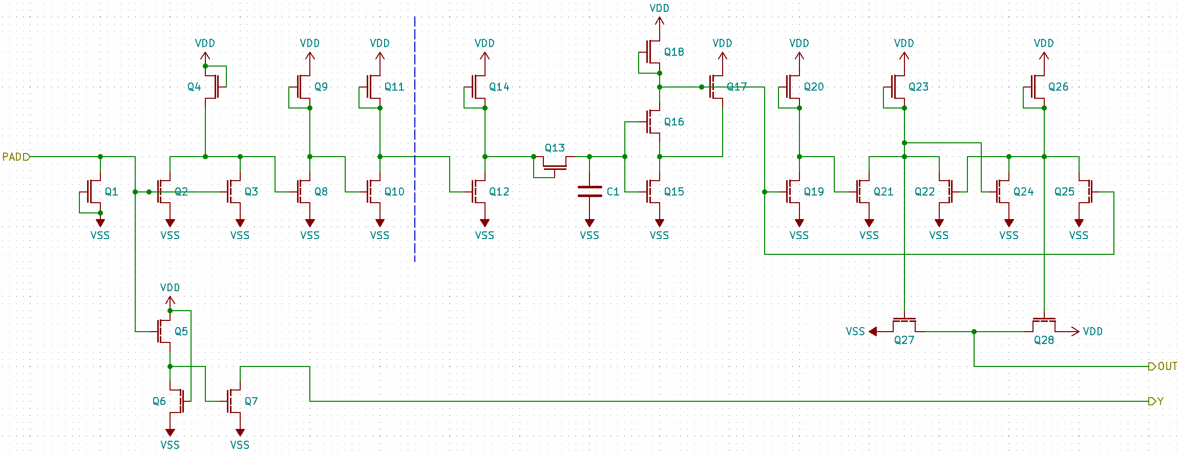
And without any further ado, here is the schematic as I see it.

Analysis
There are several very interesting bits about this circuitry:
- Why Q2 and Q3 are not one FET?
- Why Q4 has the gate connected to the drain instead of the more conventional source pin? Notably the layout assumes both options, see how metal is routed upwards without any obvious need before connecting to poly.
- The meaning of Q5 and Q6 eludes me completely. They seem to form an inverter and drive Q7, but why this arrangement?
- The Y line seems to be common among all the inputs. Whatever for?
Disregarding the baffling stuff completely, the pad itself is pulled down with Q1 acting as a resistor. Then it goes through 4 inverters in series and into what appears to be an RC filter. Q15 through Q18 form yet another weird construct which remotely looks like an inverter? After some research, this looks like an inverter with Schmitt trigger input! Q19/20 forms another inverter, feeding a NOR gate Q21/22/23. Together with another NOR Q24/25/26, it forms an SR flip-flop driving a pair of output FETs Q27 and Q28.
Overall, the output seems to be in phase with the input, no inversion.
Got any comments on the confusing bits? Would love to hear from you via mastodon or the sipron discord!
Until next time.
/DJ