Siemens M127C2
Hey sup. For a change, I thought I’d write a long post, and this is the one. Today (?) I will look at Siemens M127C2, another memory card which was used in payphones, cash cards, etc.
All silicon images were taken from here for those playing along at home.
Yeah, the M1327 turned out a bit too complicated for my level yet, so hopefully this will be an easier target lol.
Pinout and die layout
To start with, here is the lay of the land.
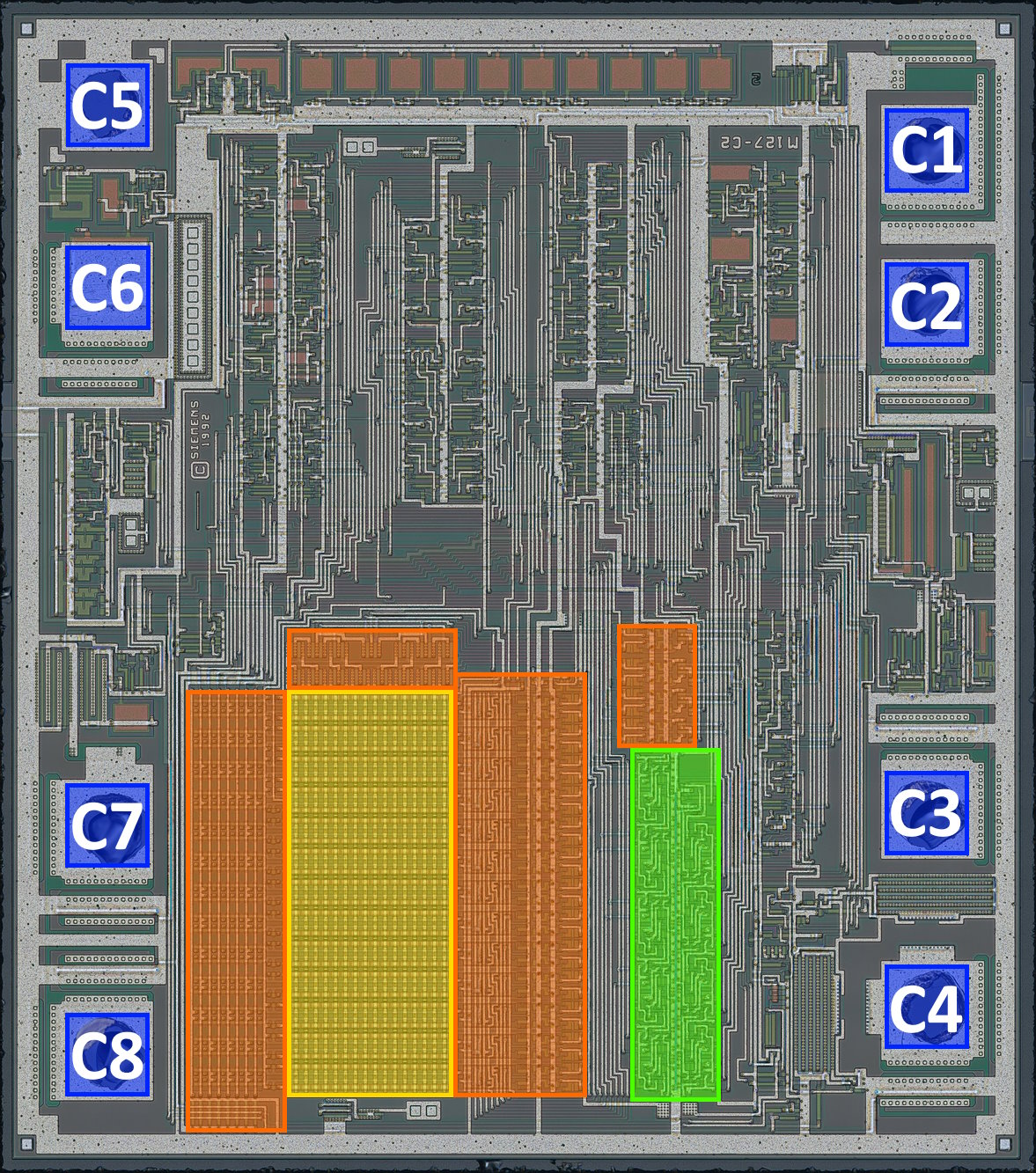
The 8 pads in blue are marked C1 through C8, like they are named in the ISO 7816 standard.
| Pad | Function | Notes |
|---|---|---|
| C1 | VDD | Power supply to the chip, +5V nom. |
| C2 | ? | RST in ISO, R/W elsewhere |
| C3 | CLK | Clock supply |
| C4 | ? | RFU/FCB in ISO, RST elsewhere |
| C5 | VSS | Power supply to the chip, 0V |
| C6 | ? | Programming voltage usually |
| C7 | I/O | Bidirectional data line |
| C8 | ? | RFU in ISO, Fuse elsewhere |
I used this page for the “elsewhere” source. Whether this specimen actually conforms to any of this info remains to be seen…
Other that that, there is the memory array in yellow and its support circuitry in orange. Some very repetitive structure marked in green. The rest of the die is taken by a variety of digital and mixed NMOS circuitry and wiring.
Notably, this device designers very rarely make poly cross diffusion without forming a transistor; will make the reverse engineering a bit easier compared to the M1327.
Pin circuitry
Starting with the obvious here. Let’s have a look at each non-power pin and try to see what’s going on.
Pin C2
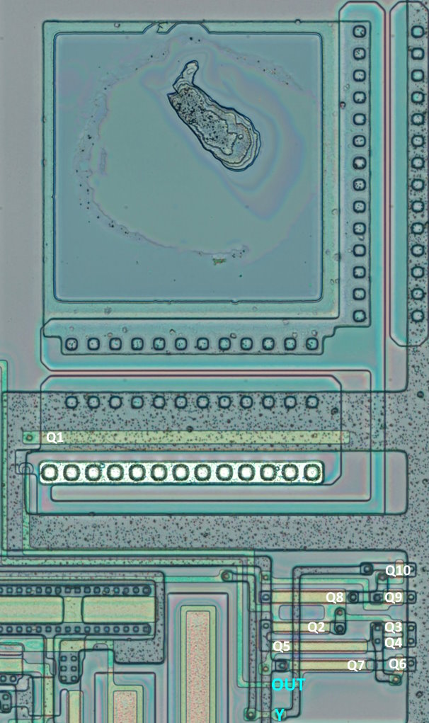
Probably one of the simplest input circuits here, here is its schematic. Very similar themes with upside-down inverters and split transistors to what I’ve seen on M1327; I wonder if the same team worked on both designs.
And its schematic:
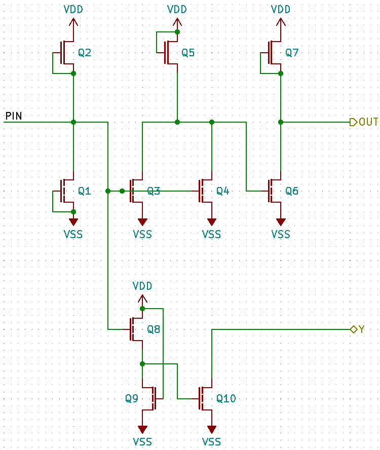
Not sure what exactly does Q1 achieve here. Q2 pulls the pin up. Then there is a chain of two inverters, Q3/4/5 and Q6/7, putting the true value of the input pin out.
The question remains on the role of Q8/9/10; they seem to be forming something with an open-drain output but as to what it does and why it is there, I hope I will be able to figure it out later on.
Pin C3: CLK
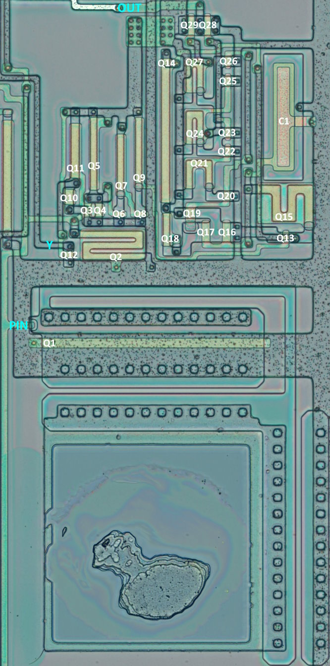
This circuit is way more complicated, although it builds on the same design.
And its schematic:
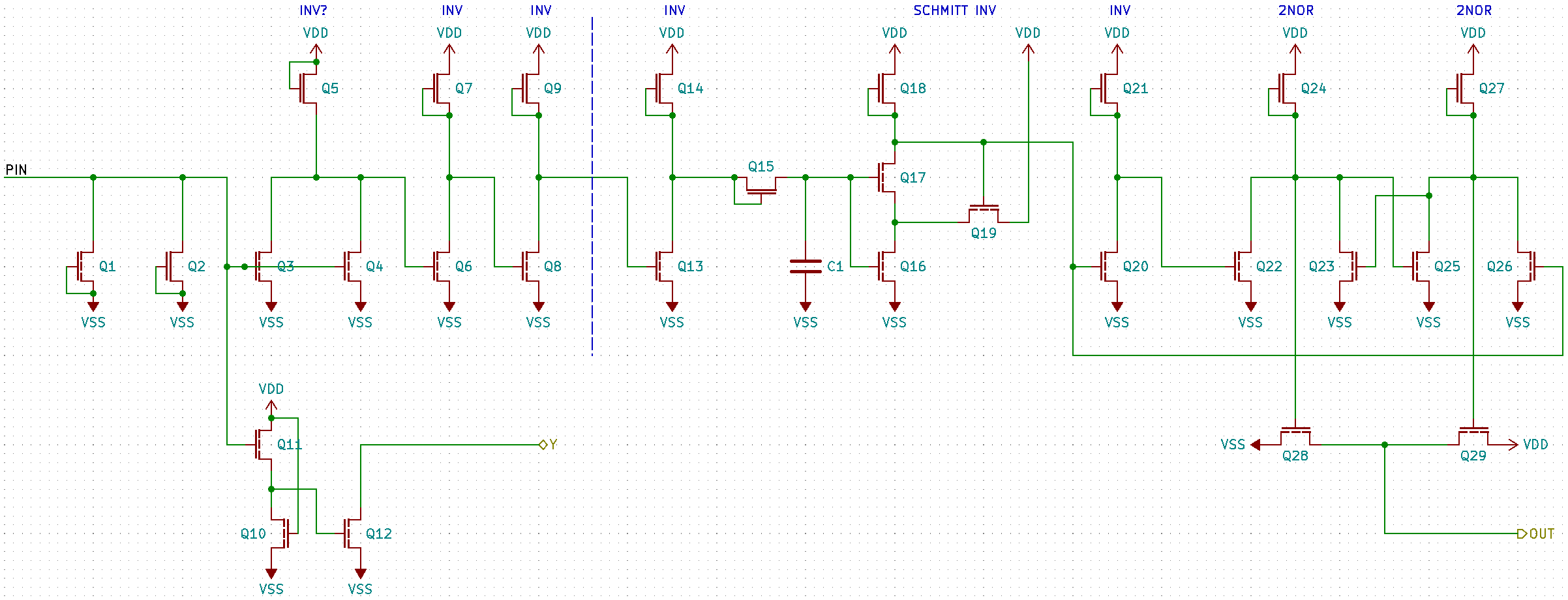
In fact, this is exactly the same as seen before in M1327. The only difference is, the raw pin connection is also used in this design.
Notably, this so far is the only place where poly crosses diffusion with no transistor being formed: look at poly between Q24 and Q25, there is ever so small
Pin C4
OK, I was wrong. This one is now the simplest input circuit.
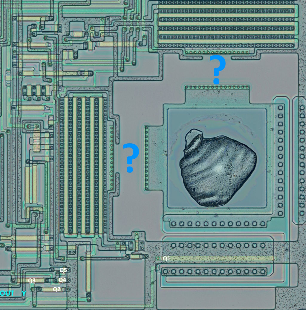
And its schematic:
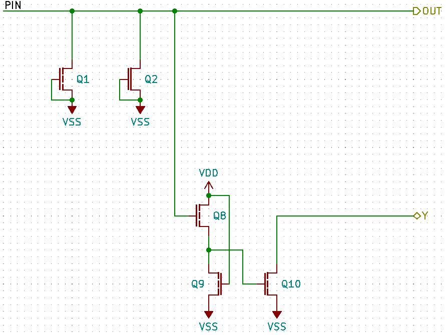
The pin drives only one input inside some logic blob; I imagine this is why it is lacking all the fancy inverter action other pins have.
There are two big questions (heh) regarding the layout – obviously something is/was there, but I can’t figure out what. It sure looks like it was connected with two poly sheets to those chonky transistors, but poly is not there any more, and no sign of it being vapourised either.
Pin C6
This is not even an I/O pad; it buggers off to a cut-off area outside the die. No wonder it was not bonded out.
Pin C7: I/O
The design of this pin is more involved.
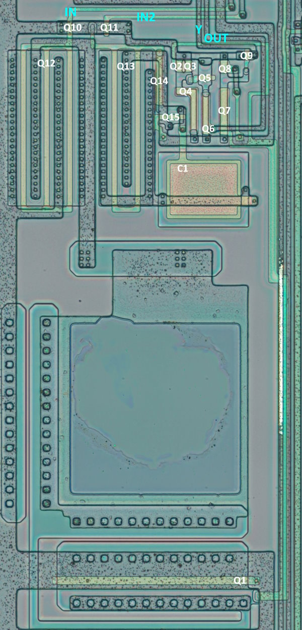
And its schematic:
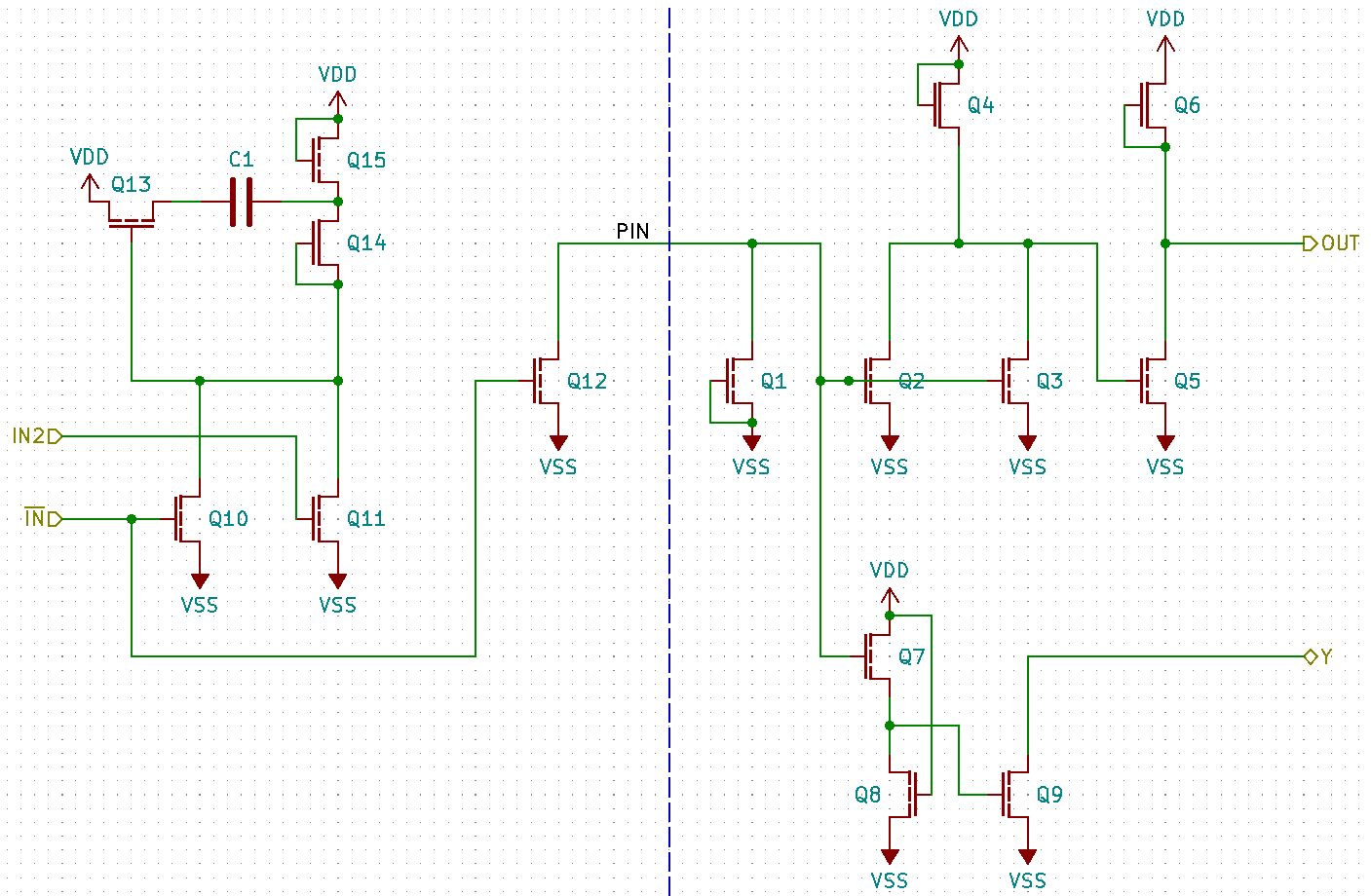
While the right hand side is the same as the rest of them pins, the left hand side makes very little sense apart from Q12. The rest of Q10 through Q15 makes no sense, it’s not even connected anywhere. Leftovers from the previous design iteration, given this is revision C2?
In any case, the input signal from the pad goes to out non-inverted.
Pin C8
The layout for pin C8 is more involved in the sense that the pin circuitry is rather removed from the pad itself.
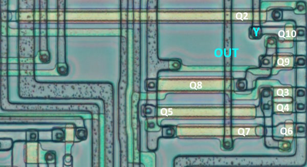
Q1 is situated by the pad itself, not shown here. Further, the poly wire from the pad goes to the other cholky transistor near pin C4.
Schematically speaking, the circuit is identical to that of pin C2.
Speaking of those two chonky transistors by pin C4, they are connected in rather funky way to ultimately nothing: input signal from pin C3/C8 drives the top of an upside-down inverter and the gate, the drain is connected to a couple more transistors and the only wire then goes to nowhere. Are these design leftovers too?
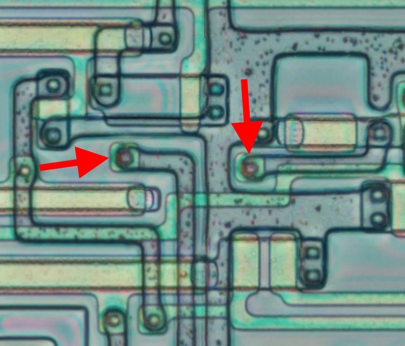
Where do all the Y’s go?
I think that’s a great question. They actually are all connected together and go in here:
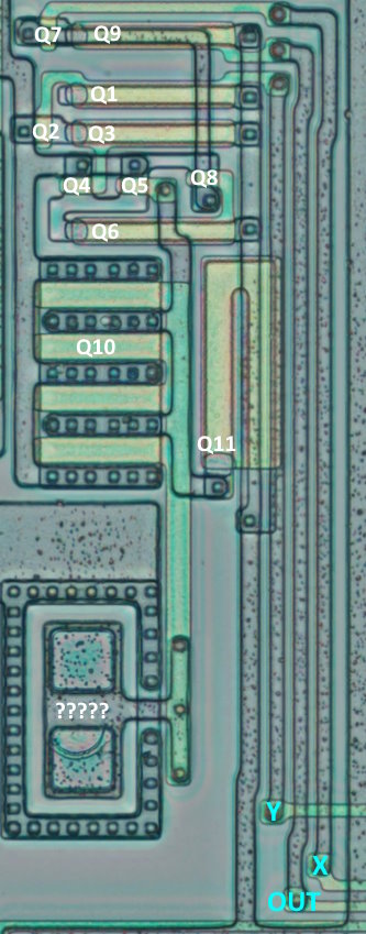
And its schematic…
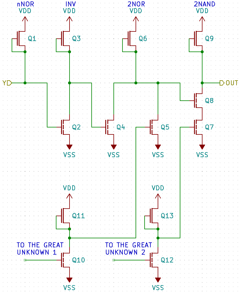
Q1 forms a large NOR gate with all those pull-down NMOS transistors in each pin circuit. Note that the point marked X on the layout connects to Q12/13 and the same funky structure that Q10/11 connects to, just on the other end of the die.
Let’s consider what this contraption might do. Say the output of those two inverters are U1 and U2. Then:
OUT = !(U2 & !(!Y + U1))
= !(U2 & (Y & !U1))
= !(U2 & Y & !U1)
= !U2 + !Y + U1
Considering that U1 and U2 connect to the same structure, whichever value they end up producing must be equal; this means the output will be set to 1 either way.
The only idea I have is, this could be a (part of) power-on reset circuitry. Hope to find out later on… I shall call this “Unit 1.”
Pump it
Speaking of unit 1, there is a funky structure right next to it. Very original, but I will call it “Unit 2a” for now. It’s hard to come up with names when you don’t know a thing. But I can see it connecting to circuitry at the top of the chip; this will bee “Unit 2b” and so on lol.
Unit 2a
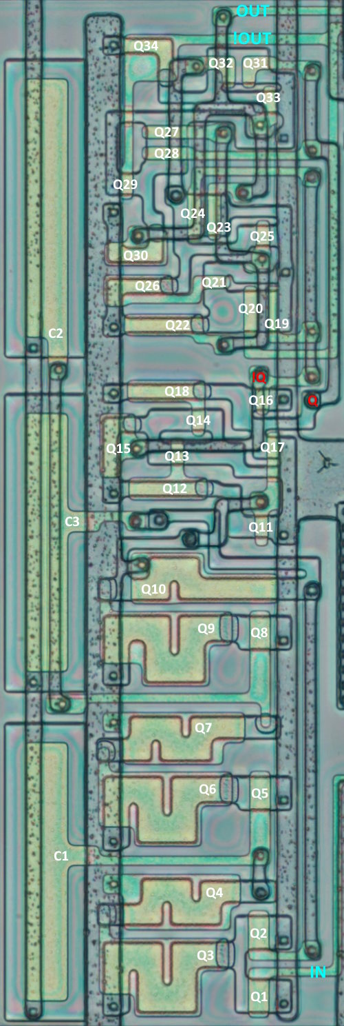
It’s a lot of circuitry to consider. Luckily, the circuit could be divided into 3 parts. Here is part 1 of the schematic:
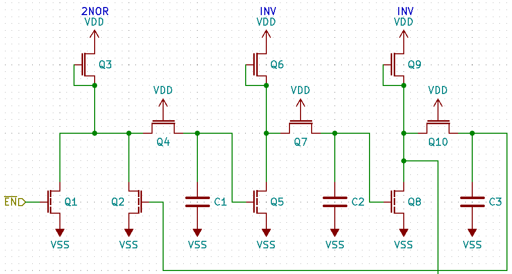
This looks like a chain of inverters with RC filters between them. It’s a ring oscillator with an enable input! Consider what happens when !EN is H: gate 1 outputs L, gate 2 outputs H, gate 3 outputs L, and that is fed back to gate 1 – but its output does not change. Now when !EN goes L, gate 1 will output H while Q2 gate is still at L; this will propagate through the inverter/RC chain and eventually Q2 gate will be pulled H. This will repeat again and again, resulting in an oscillation which is tapped at the output of the last inverter. This then goes to part 2:
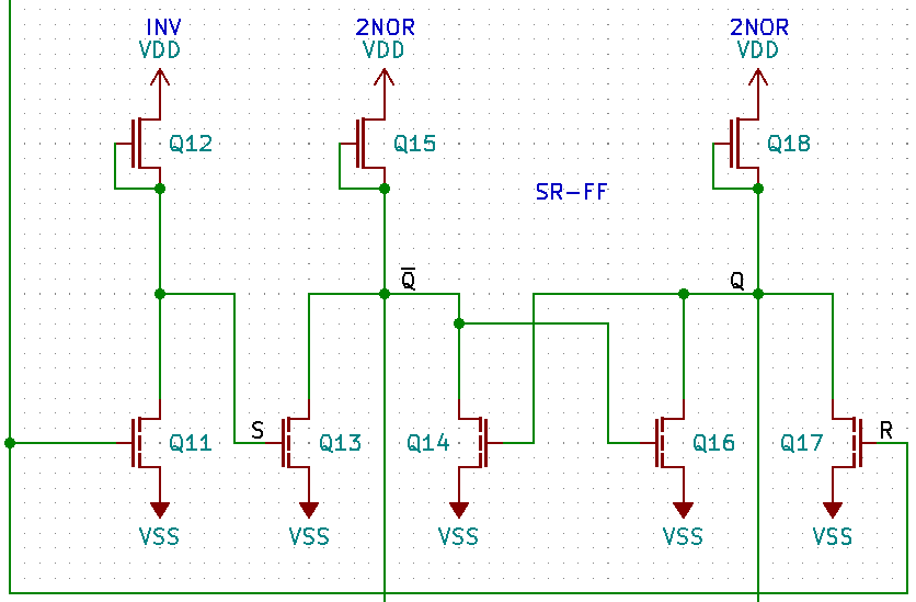
…which is an SR flip-flop with an extra inverter at the input. This splits the input signal into its true and inverted copies. When !EN is negated, Q is H and !Q is L. These are fed forward to the next and final part:
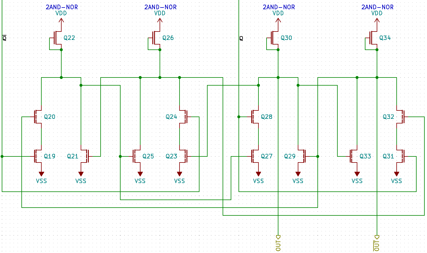
Believe it or not, these are two SR-type flip-flops but with an enable input each. Enable inputs are connected to one of the AND stack transistors and are controlled by the outputs from the previous stage; when enable is at L, the flip-flop keeps its state. Without going into too much detail, this looks like a primary-secondary arrangement, where outputs are flipped on one phase and copied over on the other. Not sure it is as important to understand which is which, as the circuit outputs two square waves 180 degrees apart exactly and without overlap.
These outputs are then routed towards the top and into a funky circuit above pad C6 which does not appear to have any output, again, and then into the circuitry at the very top of the die.
Unit 2b
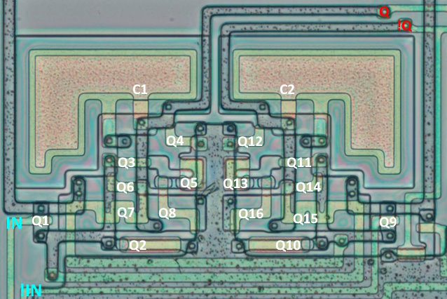
In Unit 2b, we have a lot of funky. This will come in two parts, and here’s part 1:
And its schematic:
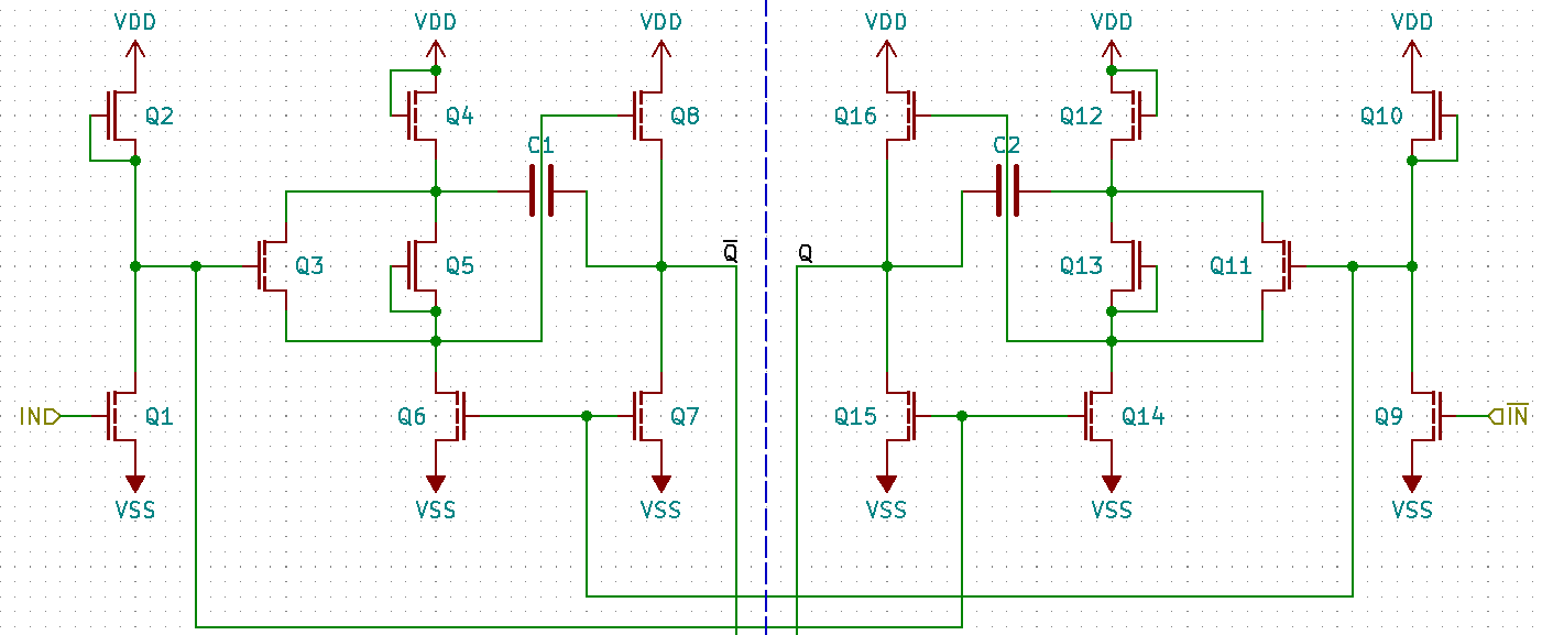
Like said before, this is fed with two square waves 180 degrees apart. Suppose IN is H and !IN is L, then the Q1/2 inverter outputs L and the Q9/10 inverter outputs H. Q3 and Q8 are off while Q6 and Q7 are on, pulling !Q to L. Conversely, Q11 and Q16 are on while Q14 and Q15 are off, and Q is at H. So each half outputs the inverse of its corresponding input in a push-pull fashion. I am not exactly sure about the role of Q4, Q5, C1 and their mirror countrparts.
These outputs feed into part 2:

And its schematic:

There is a long chain of FETs and capacitors here. Let’s see what’s up.
Suppose we start with all caps discharged and both drive inputs at L, then VDD is applied. This gets Q17/18 to conduct and charge C3 to voltage +5V (optimistically, okay), with the bottom terminal positive. Assume for now this does not propagate any further to C4 and beyond. Now Q goes from VSS to VDD and !Q stays at VSS; this means the top terminal is now at +5V and the bottom terminal at the sum of +5V and the voltage across C3 – going to about 10V. Q17/18 now can’t conduct but Q19/20 can, and C3 and C4 connected in parallel now share the charge and settle at +5V each. When Q’s flip, C3 begins to recharge from VDD; top terminal of C4 is now at VDD so the bottom terminal raises to the sum of +5V and the voltage across C4 – again about 10V, and spills that over to C5, settling at +5V each. Now, the Q’s flip again; this time, C3 and C4 are both at +5V initially. The bottom terminal of C3 raises to +10V, but now C3 and C4 settle at (10+5)/2 = 7.5V each. And so on, and so on. I’ve created a simulation of this circuit to verify this thinking, and it seem to check out; the Nth capacitor is pushed to theortical (N+1)*VDD volts, however I doubt this is reached in practice. Theoretical voltages are VOUTA=35V and VOUTB=55V.
In fact, this looks exactly like the Dickson voltage multiplier design.
Unit 2c
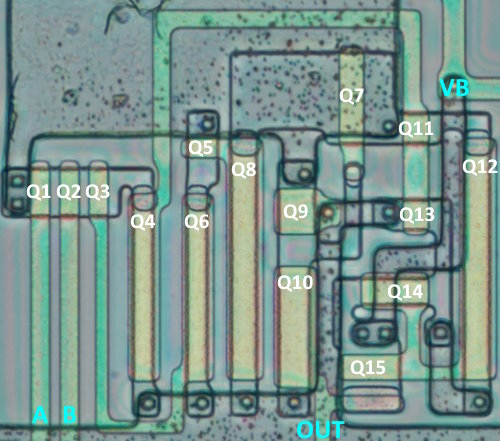
VOUTB also connects to a piece of circuitry right next to Unit 2b, say this is Unit 2c.
And its schematic:
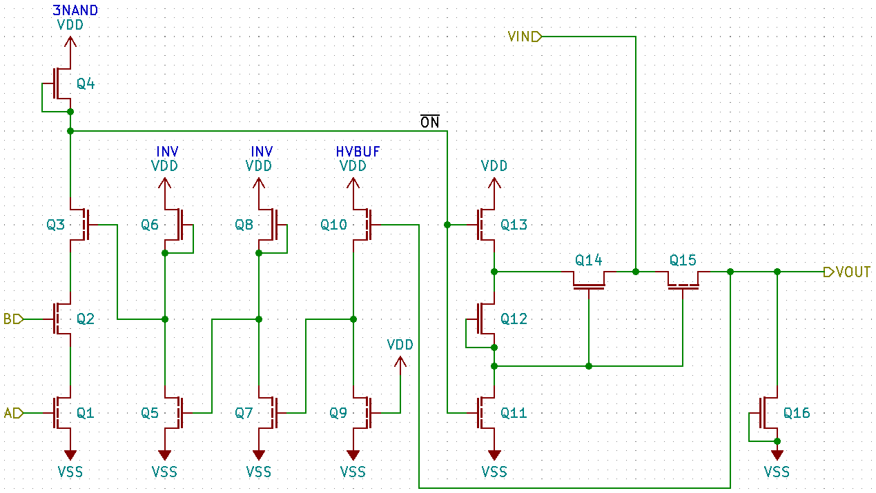
Note: Q16 is way off and not shown on the layout.
The output of 3NAND can be H or L; assume it is H for now (some of Q1..3 are not conducting). This means Q11 and Q13 start conducting, then current flows through Q12, developing a voltage close to VDD across it. This closes Q14 and Q15, so the output floats. When the output of 3NAND is L, Q11 and Q13 won’t conduct but Q12 and Q14 still do. This pulls the gate of Q15 to VIN, and thanks to the Q16 load it starts conducting thus passing the voltage to the output. This part looks like a pass transistor with an inverting input…
What I don’t get is how this is supposed to be controlled. When the pass transistor is off, the low level passes through the inverters and shuts down Q3. Now no matter what the inputs are, it is not possible to do anything. If the buffer is inverting, this would make sense circuit-wise – but how does it do that? Q11..15 is inverting, after all.
Unit 2d
Two high voltage wires terminate at the next unit, Unit 2d. Here it is.
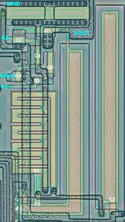
And its schematic:
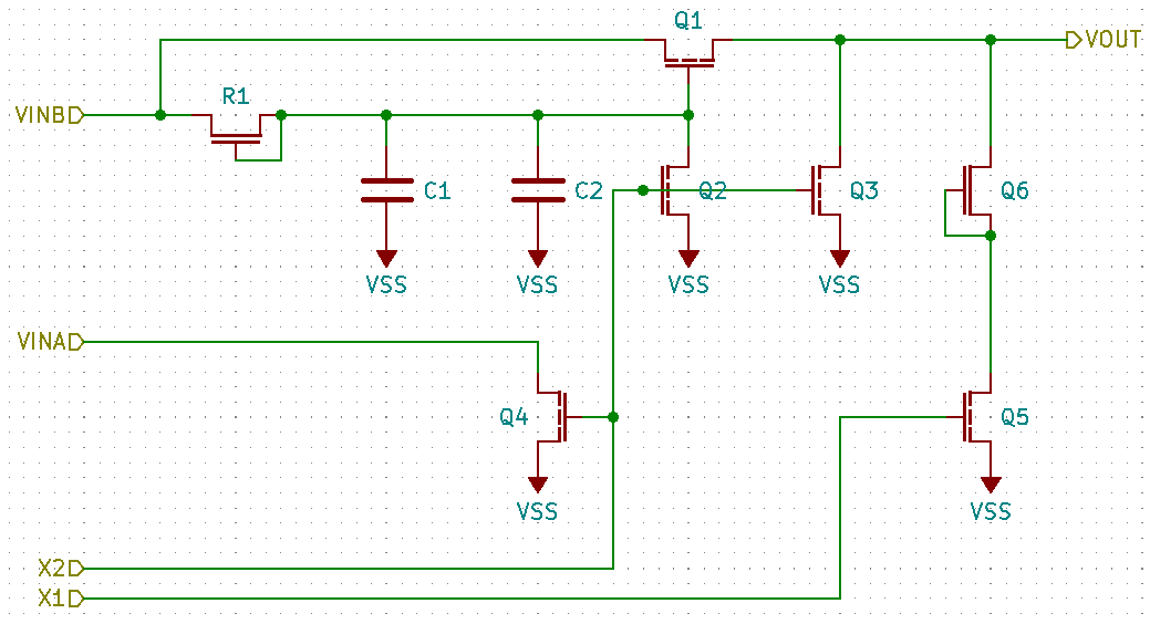
R1/C1/C2 form a delay circuit, which opens Q1 after some time when VINB is applied. Q2 and Q3 apparently serve to shut the high voltage down? Same for Q4, though it seems to short the VINA to ground and that’s it? The routing of Q3’s VSS side is very odd, going to a dedicated wire and then to VSS instead of connecting directly to VSS that’s already there… What does Q5/6 do is a mystery too – maybe a way to slowly discharge the voltage?
…WRITING IN PROGRESS