Philips V83C851V0 ROM: internal details
Hey there. It has been a while since the last blog post. These days I do simple die walk-arounds on Mastodon without writing down anything much, but today will be an exception. In addition to the die tour of this specimen, I will note down more details on how the ROM is implemented on that die. A blog post looks like a more fitting form for that, so “without further ado, let’s get right to it”.
The chip in question is a 80C51 derivative created by Valvo/Philips (which is why it is V83C… I suspect, like other chips in the same family). Typical for 8051s, this includes 4 KiB of internal mask-programmed ROM. Here is an overview shot of the whole die to show its location.
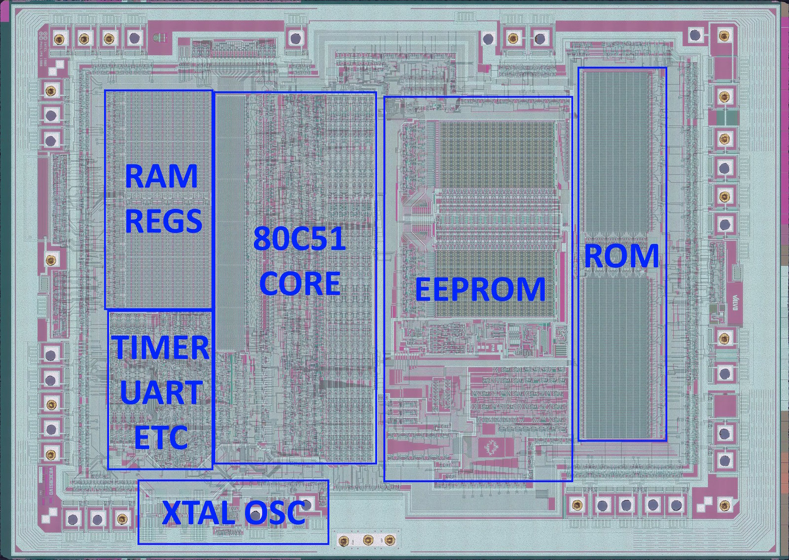
Given its stated capacity, I would expect there to be 12 address lines coming in and 8 data lines coming out. Without going into details of the 80C51 core implementation, which is a topic for another time, these signals were located on the die and sure enough, A11..0 and AD7..0 are routed to the unit. It is not too hard to do given alternate functions for each pad. Address bits 11..5 are used for row selection, and 4..0 for column selection.
Column decoding/multiplexing
Let’s have a look at the column multiplexer.
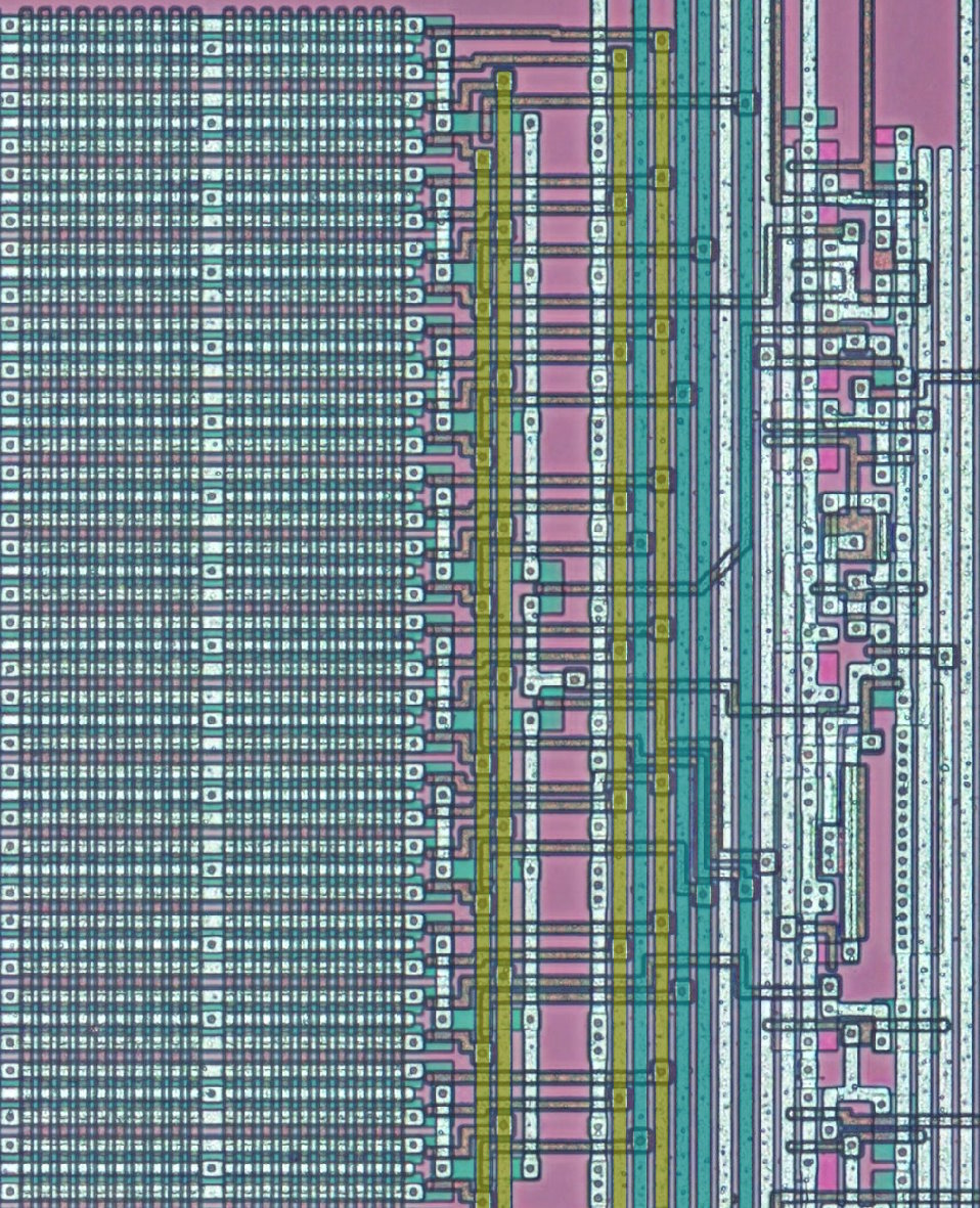
Situated between the bit plane on the left and the sense circuit on the right, this circuit is a tree of pass transistors controlled via multiple lines being decoded lower address bits. Its job is to select one of the 32 bit lines (here horizontal metal) to produce an output bit value. The circuit is replicated for each of 8 output bits. Four lines (painted in olive) drive the first level of 4 selector transistors, then four more lines (painted in teal) select one out of four 4-line blocks, then finally two transistors choose one of those; 4 * 4 * 2 = 32 so everything adds up here.
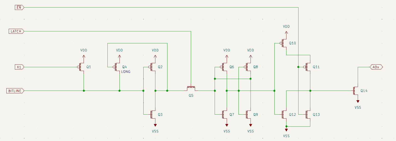
The sense/driver circuit is a series of an inverter-amplifier, a latch, and a NOR gate driving the open-drain output. At least some signal semantics could be derived from the schematics.
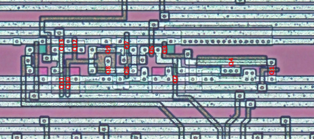
And its transistor locations:
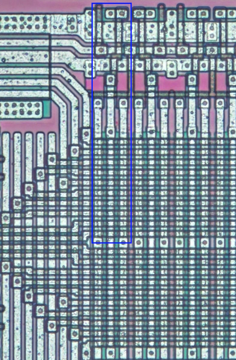
Row decoding
Now for the row decoding:
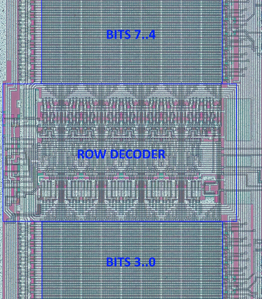
It is wedged right between the two bit half-planes and makes use of the higher address lines to select a corresponding word line. Note there is a slight irregularity: there is what looks like 8 of the same circuit replicated and then a smalller piece of a different design.
An astute reader would have likely noticed that hey, something is off here. If you count word lines (in poly) running through the bit plane, there is 90 of them total, 10 each per 9 chunks. This doesn’t mesh well with the 4096 bits stored per each output bit, which gives 4096 bits / 32 bit lines = 128 word lines. There is either too few bits provided by the design, or something funky is going on. It’s the latter, of course.
Let’s have a closer look at one decoder slice:
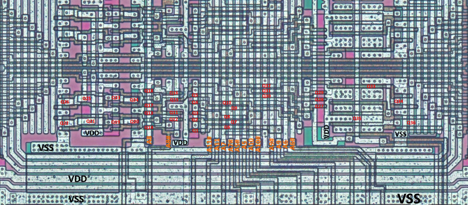
In fact, there are two separate circuits in each slice. One type of them decodes address lines A7..5, and produces outputs routed with metal tracks around the decoder unit. Each slice produces one of the 8 decodings of those 3 bits. Note the circuit has an active low output!
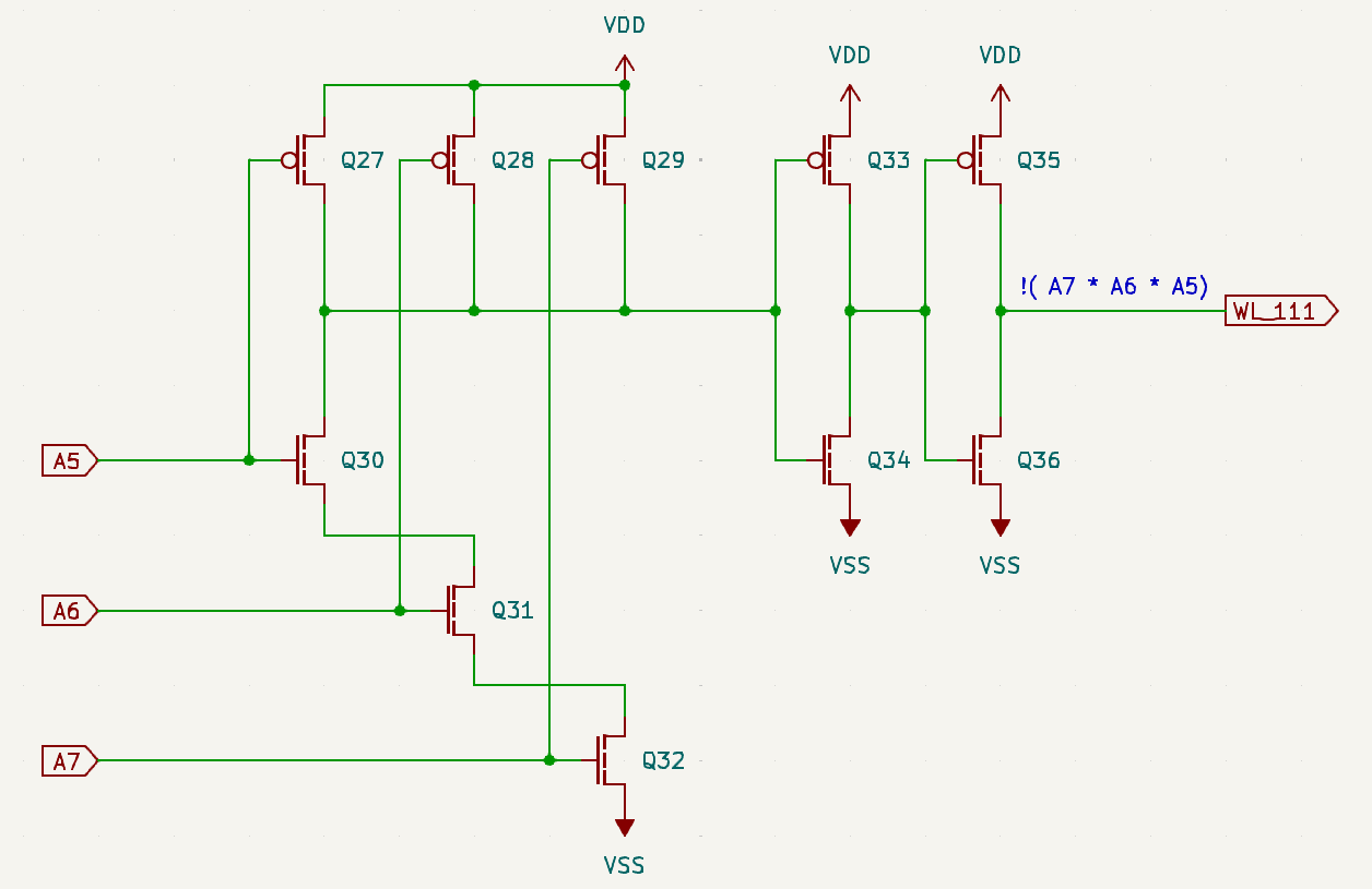
Each address input can be connected by a via to either true or inverted address line, making layout reuse easy. The circuit shows all true connections.
This takes care of 8 word lines per chunk, what about the other two? These are produced individually per each chunk by this circuit:
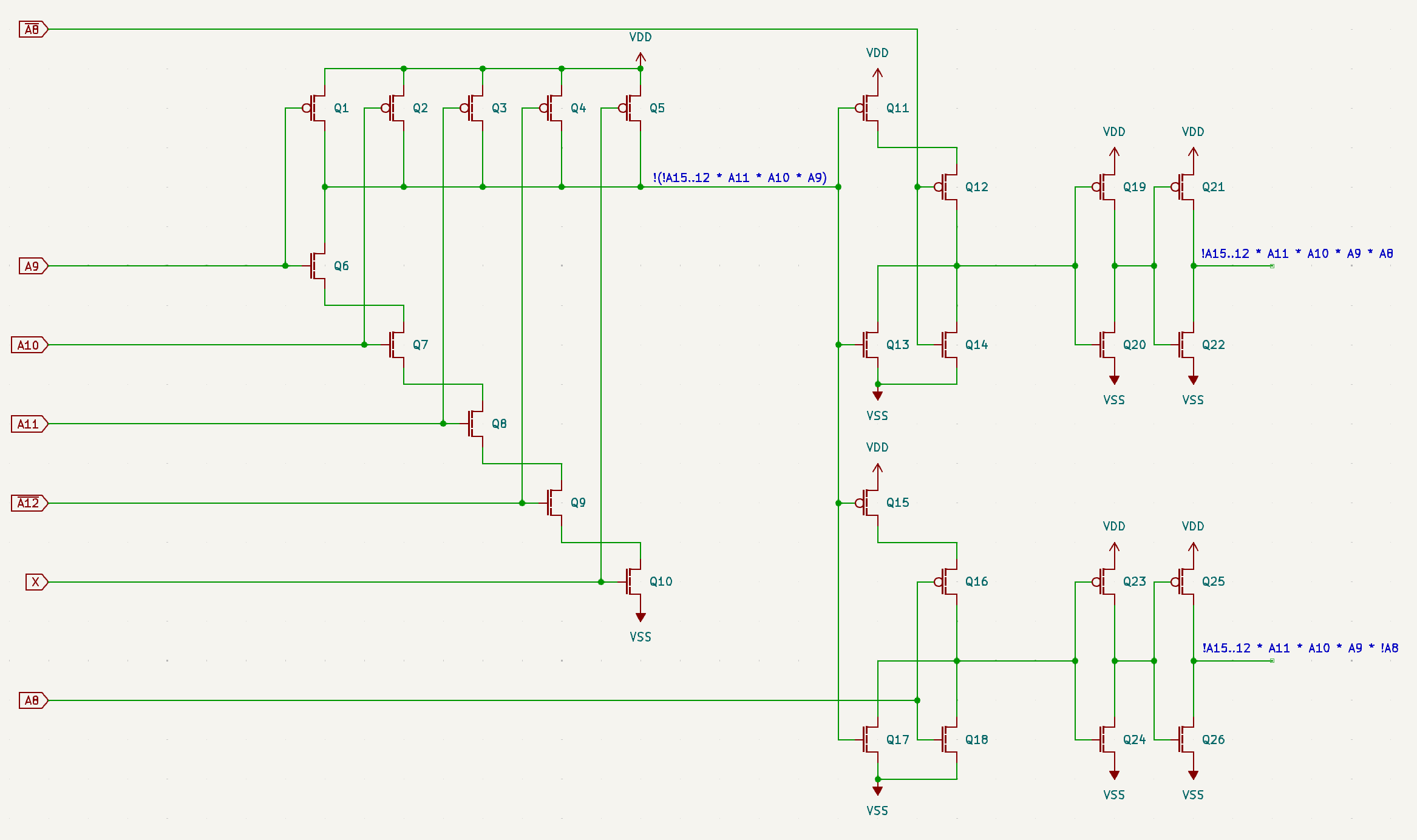
Like before, specific activation values are programmed by appropriately placed vias for lines A11..9. The mystery signal X is likely either ROM select or just the rest of the high address bits set to zeros. The two outputs produced are activated when the programmed address value is received, also taking into account A8. Note that unlike word lines, only one of these “selection lines” will be active for a given memory address.
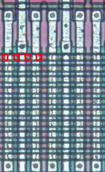
Bit transistors
Let’s have a closer look at the actual bits now. Specifically, consider this piece of the bit plane.
At the top, two PMOS transistors drive the two bit lines, and one NMOS transistor drives the ground line between them. All of these transistors are driven by the same line, so when one is active, the others are not. I believe this is the implementation of the precharge circuit, pulling all the bit lines high before the actual read starts. Otherwise, it would make little sense to actively pull all lines high all the time as you won’t be able to read anything. According to books, another option seems to be passive pull-ups on each line.
You may be surprised to learn that the rest of the rectangle, where it is more dense, somehow contains 40 transistors, 10 each in 4 blocks.
This is likely the most dense area of the whole design, with transistors being super small and packed tight, probably at the limit of the process. Schematically, this is what it looks like:
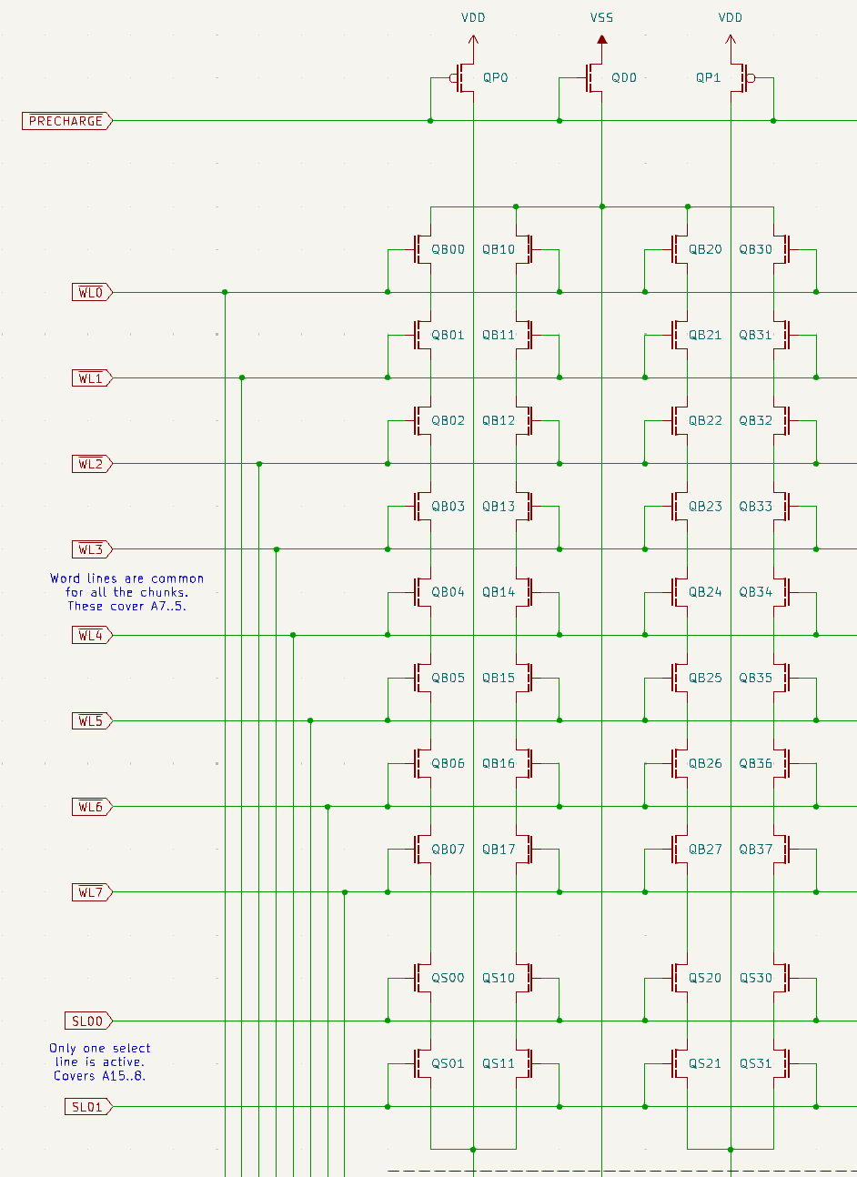
This looks like a NAND organized memory with some tweaks. As a reminder, NAND memory string works like a big NAND gate. Suppose you want to read the state of QB04. For that, you need to pull all the word lines high, so all the transistors in other word lines conduct and can be disregarded, and pull the WL4 low. If a transistor is present at QB04, the bit line will remain high; otherwise, it will be pulled low. Presence or absence of a transistor is what makes memory programmed.
While the schematics shows QSxx all populated, in reality there will be only one in each vertical string, so SL00 will activate QS00 and QS20, for example, and SL01 will activate QS11 and QS31. With available images, it is not possible for me to tell which ones are populated. But they make sure that only one string of NMOS transistors is connected to each vertical bit line, providing additional address decoding kind of in place.
And that’s it, that’s the trick. You can think of each bit line having double the capacity.
One question remains, why is there 90 of these word lines. This in fact hints at there being more memory than the 4 KiB announced in the data sheet, selected by that different bit of circuitry. For the moment, I do not have confirmed information on how to access it or what it stores; more reverse engineering work is needed. And yet another can of worms is the control logic for the ROM…
Until next time! /DJ