Detailed look at PLA architecture in NEC V20
Oh wow, it has been a while, really. I should start writing more again, but energy is scarce and the winter is coming… Maybe that’s a good thing, we shall see.
This writeup will go into some depth on the particularities of programmable logic array (PLA) as found in the NEC V20 (uPD70108) design. This is a follow-up to @gloriouscow’s inquiry on the topic.
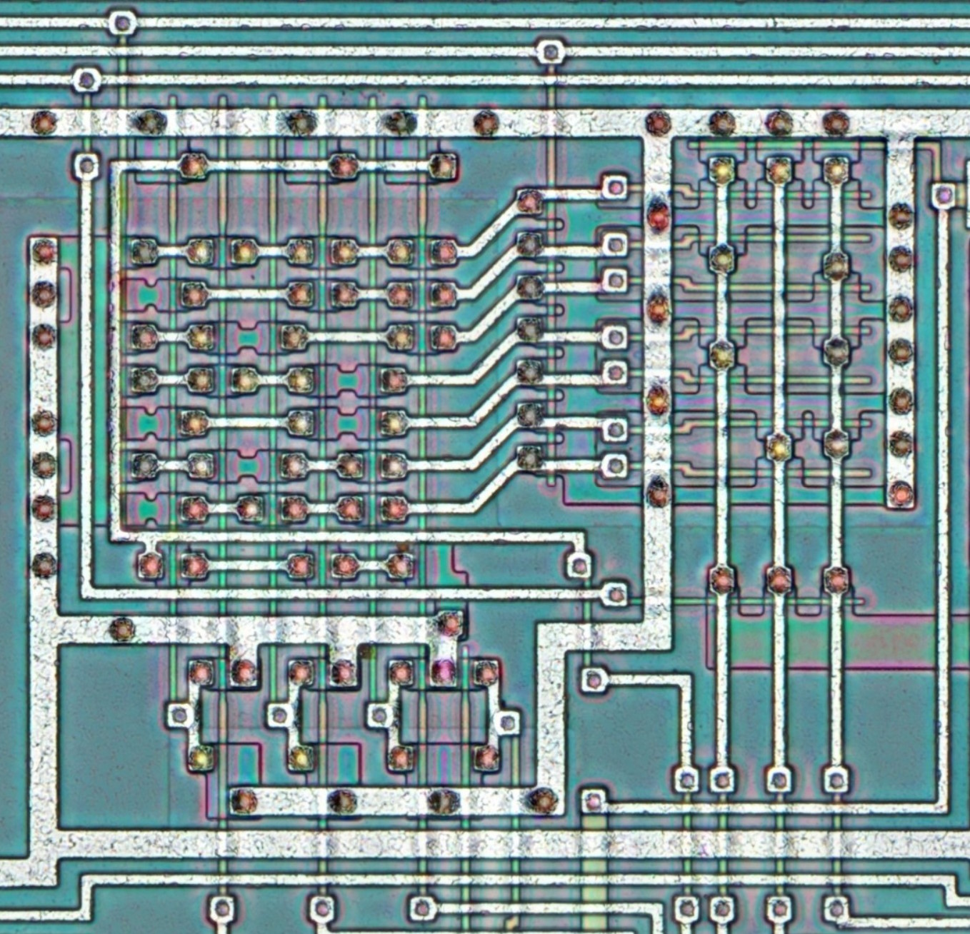
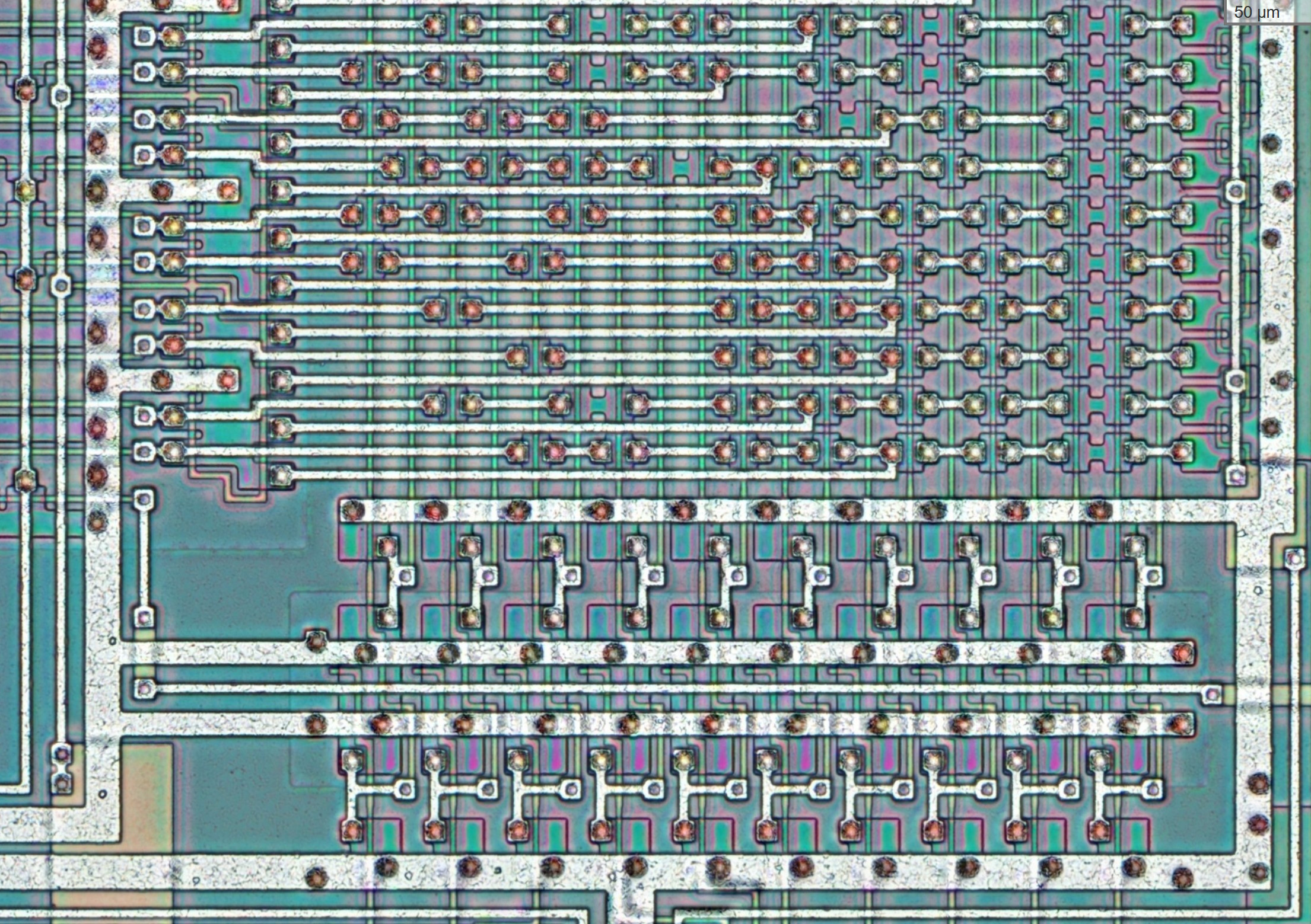
There are only 9 PLA structures on the die, including the microcode storage. The overall structure of these PLAs appear to be similar enough to consider a single example.
As a reminder, PLAs are useful when you have a set of input signals and want to produce a set of outputs which are arbitrary combinatorial functions of (sub)sets of the inputs. These can be expressed as either a sum of products or a product of sums. One can switch between the two forms without issue; I will stick to the SoP naming for the rest of this text.
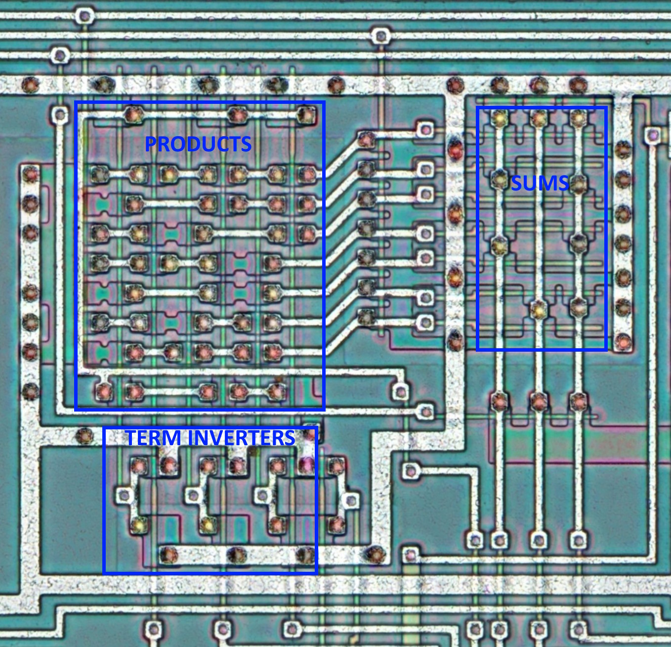
Here, there are only 3 inputs which are passed through 3 inverters to obtain a complement of each input. The 6 signals are then fed into the product matrix producing 7 products. The products then are fed into the sum matrix, producing sums of said products. Easy peasy so far, this is how any PLA works. The eagle-eyed reader will have noticed, however, that there is more going on than just that. There are extra signals and transistors in both matrices. What is that about? Let’s draw some schematics to try and answer the question.
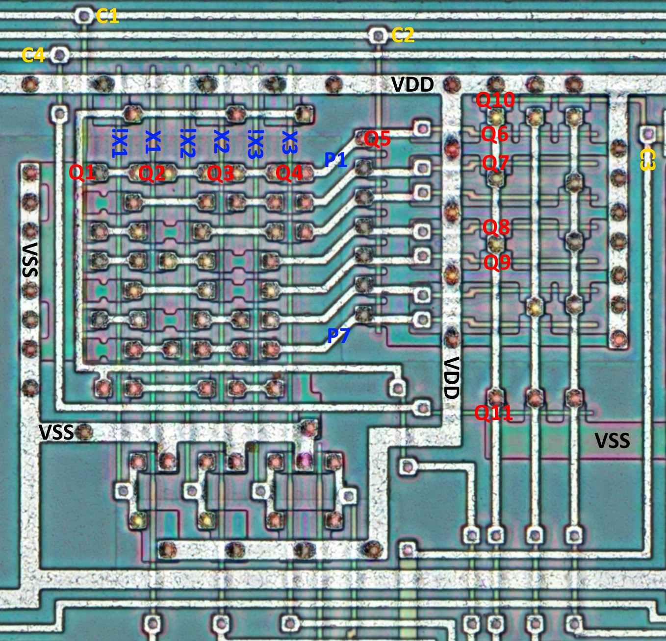
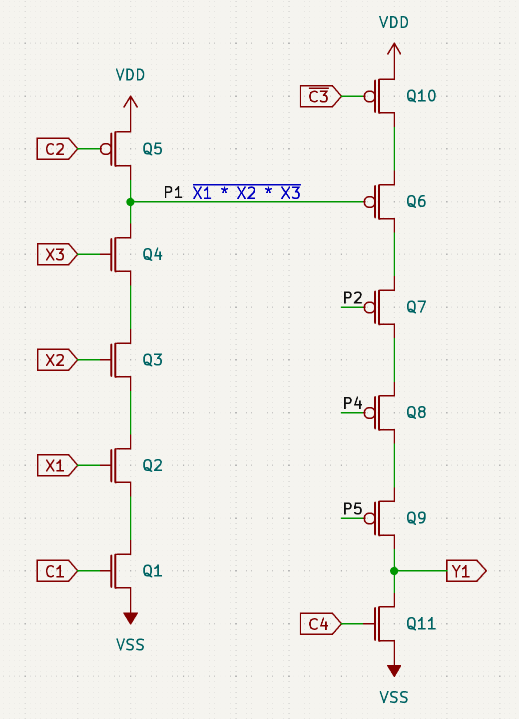
The schematic view shows clearly what is going on with the products. The left side looks like a simple NAND gate, were it not for Q1 and Q5. C1 driving Q1 acts like an enable signal; if it is negated, then no combination of inputs will affect the output. C2 driving Q5, though, does something else: necessarily out of phase with Q2, it pre-charges the output line – as well as the all the transistor gates in the sum matrix – to VDD. So when C1 is asserted as well as all the inputs, the whole stack of Q1..Q4 would pull the line low; otherwise, the line floats and retains the charge for some time. This design totally relies on the facts that a) each product line has at least some capacitance and b) FET off-resistance being high enough not to drain that capacitance too soon. This is why this CPU has a minimum clock frequency.
Now have a look at the right side, forming sums. The idea is exactly the same, only everything is inverted. C3, active low, needs to be asserted to produce the outputs, and C4 pre-discharges the line. Each of the sum terms need to also be active low: Y = !P1 * !P2 * !P4 * !P5 = !(P1 + P2 + P4 + P5). Assuming the inputs before inverters are active high, we get a sum-of-product output active low.
Now, why did they choose such a complicated, dynamic design? One of the reasons I can imagine is like this. In an NMOS process and using a textbook approach, designing a PLA is easy: you have your NAND input stack and one single depletion pull-up to produce each product. But you can’t do that in CMOS: were it a functioning gate, it must have equal number of NMOS and PMOS transistors. It looks challenging to produce such a structure and retain all the area saving benefits of PLAs; looking at how sparse this design is, that would be a major hit. But the dynamic approach appears to emulate NMOS benefits and allow a “simpler” design using the same technique, at the cost of extra clock inputs and an added requirement of a minimum clock frequency.
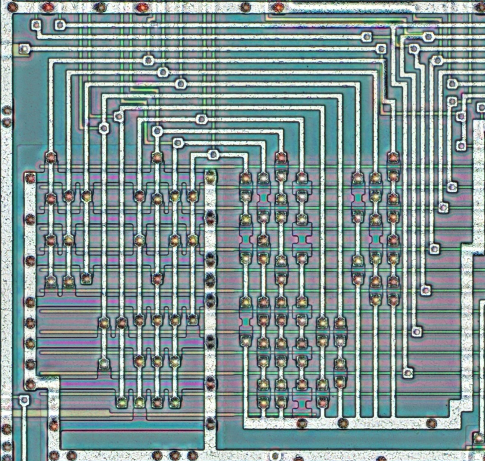
But wait, there is more. Consider this one:
The structure is very similar, and the sums matrix itself (on the left, cropped off) is unchanged, from what I can tell. The products matrix, however, is slightly different. For each product, there is an extra metal trace going in the middle! What’s up with that?
I do not know for sure, but I can make an educated guess. I think this also has to do with how pre-charging works. They might not had enough voltage to quickly and reliably turn all the FETs in the stack relying only on the charge stored in the product line. So they choose to pre-charge another piece somewhere in the middle, to allow those transistors to see higher Vds and thus have lower resistance when their gates are pulled high.
There are other variations on the theme. One of PLAs has product line precharge on the end of the lines, so moved all the way beyond the sums matrix. And, amusingly enough, there is a static PLA design too. Notice how each input term runs through transistor pairs – and this produces products only, clearly taking a hit on the area consumed:
My conclusion is: the analysis of PLA functions on this die can likely disregard the dynamic quirks and concentrate solely on products and sums. Extra circuitry does not impact the functions generated.
Until next time!
/DJ