Siemens M1327A3, part 4: TFF chain 1
Ahoy sailor, today I shall continue the exploits against Siemens M1327A3. In this post, I will look at the three counter chains I mentioned in the previous part. Here is where they are located on the die:
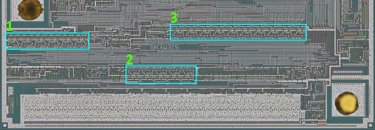
Without further blab, let’s get started with chain 1.
Chain 1
This chain has 6 T flip-flop (TFF) sections plus some more circuitry around them; one is directly above (red) and connected to the outputs and the other is to the right (yellow).

This is what I already know, put into a schematic:

Sorry, but most of the schematics here will be backwards (right to left) so as to stick to the orientation on the die.
Above each chain link, I see three transistors arranged in the same way: two to the flip-flop outputs and one to the ground. Let’s put them on the schematic.
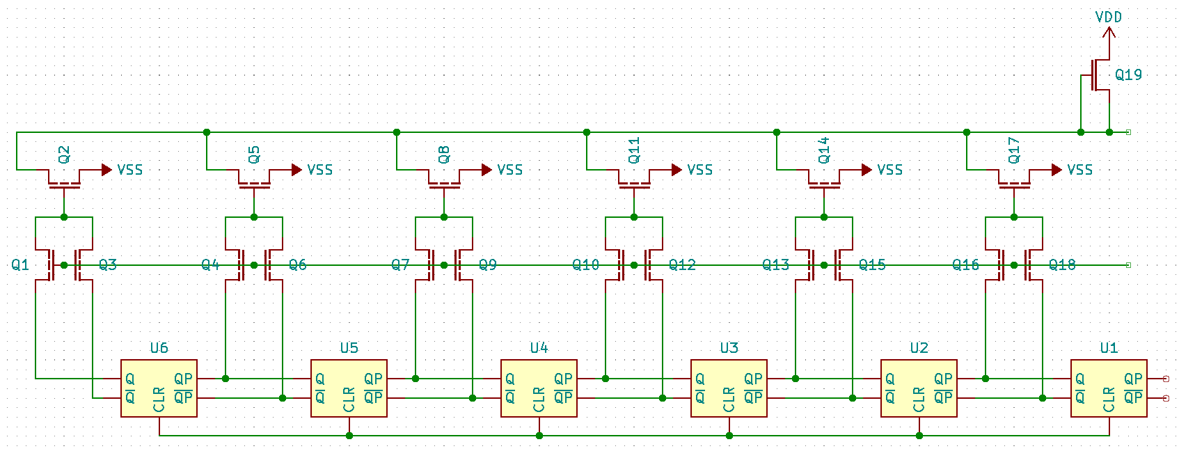
A peculiar arrangement. Again, some of the transistors there are real, some are not; “missing” transistors always conduct. The line controlling pass transistors Q1/Q3 etc comes from outside the counter unit; I’ll mark this as input X1. Tracing the common wire for Q2 etc, I can see it connects to a depletion-mode MOS thus making all of them into a big NOR gate. This means the output will be logic high only when all of the pull-down transistors are off. If anything, this looks like the “compare” function to turn this binary counter into a modulo-N counter by choosing which pass transistors are implemented. Let’s update the schematic by removing fake transistors and renumbering existing ones.
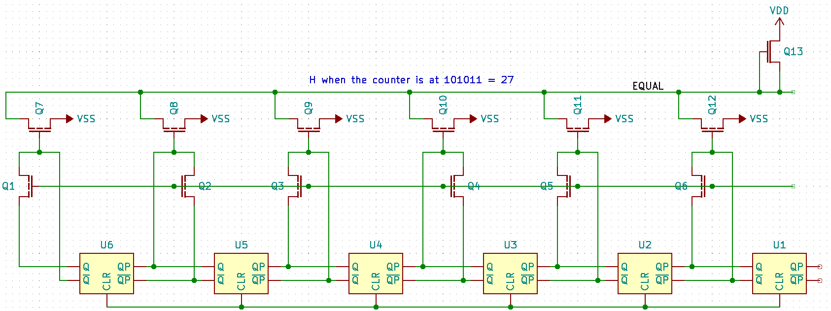
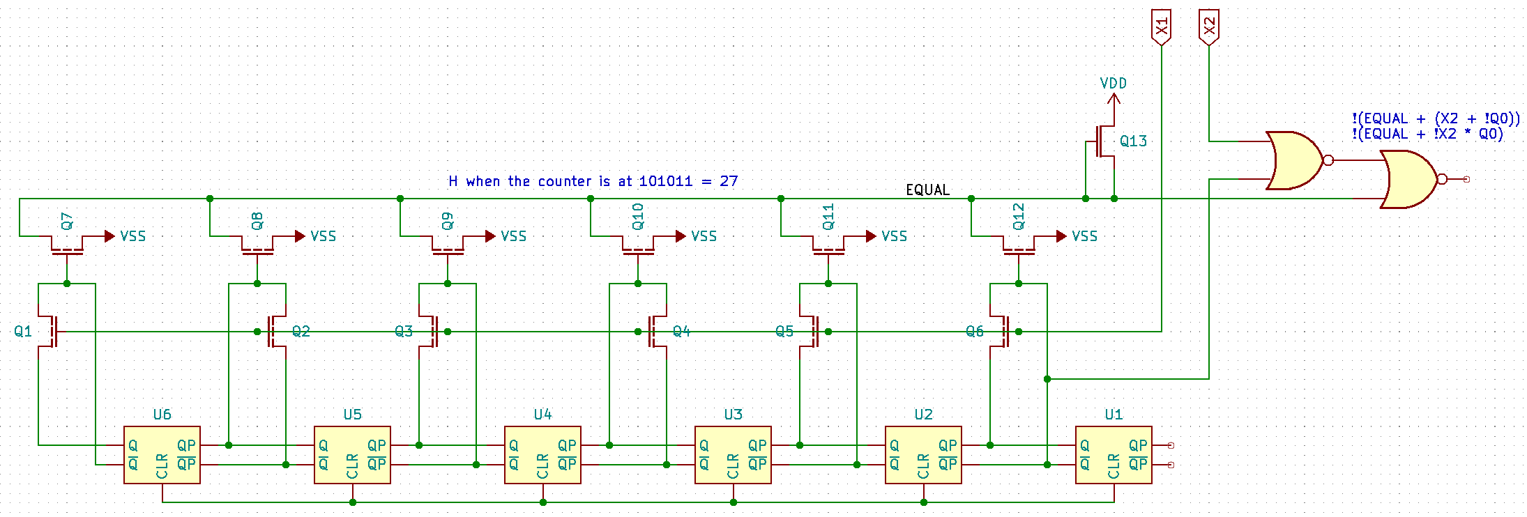
Now I want to trace the EQUAL signal; it only goes into a NOR gate in the yellow area and stays in that area, going around in semi-circle. It also takes in another input from outside the unit, marked X2.
Up next, let’s have a look at how the actual pair of clock signals is generated for this counter. This means reverse engineering most of the yellow box stuff. And, oh. my. satan! is this complicated. 40 transistors joined in a convoluted electric spaghetti. In addition to Q/!Q, the circuit blob outputs the clear signal (also outside the unit) and takes two more inputs from outside, X3 and X4.
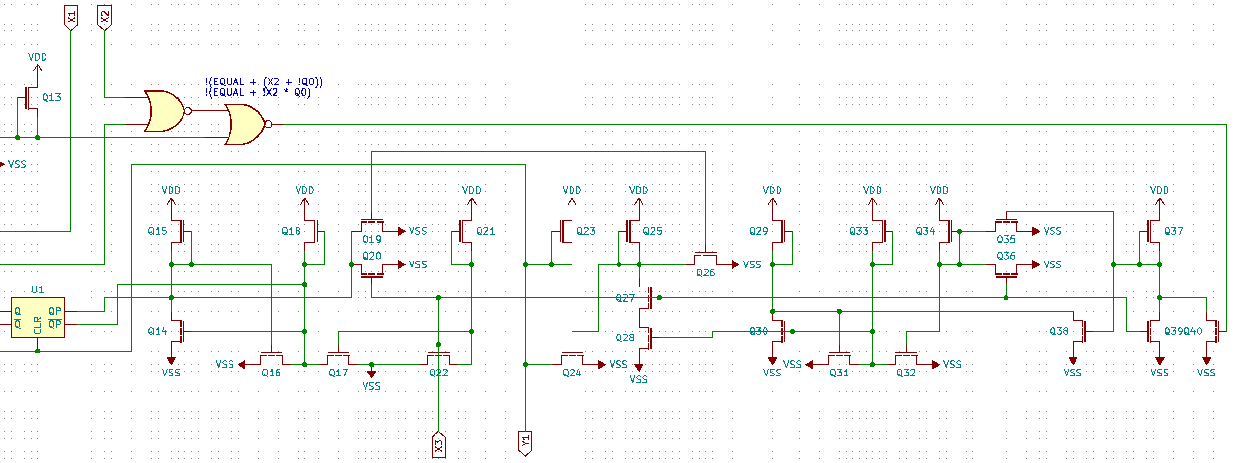
And the markup of where these transistors are located so that I don’t lose my sanity:
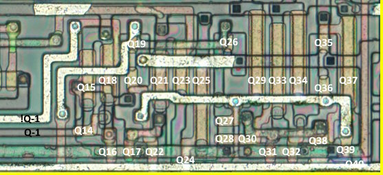
After some shuffling around and double checking, this actually started to make some sense. At least, no obvious errors.
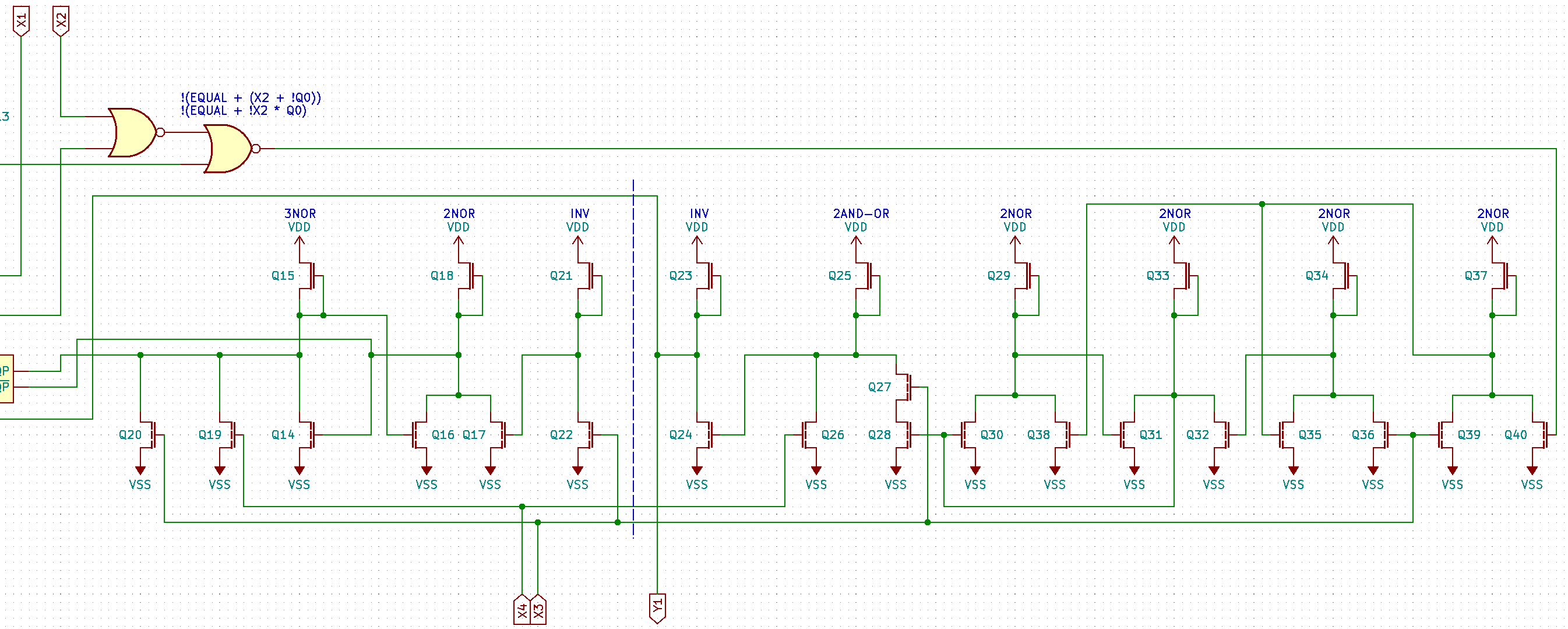
The circuit comes in two distinct parts, one driving the clear signal and the other driving the input pair. I have redrawn the clock part using logic gates instead of transistors:
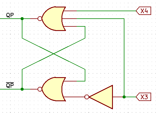
Clock driver analysis
First, if X4 is H, then QP is set to L irrespective of anything else. If X4 is L, then operation is only affected by X3.
If X3 is L, inverter output is H, setting !QP to L. All three inputs to the upper NOR are L, thus QP is H.
If X3 is H, then QP is L. Inverter output is L too. Then, !QP is H.
This effectively splits the X3 signal into two phases in a complicated way. This X3 now looks like the actual clock input, allowing the counter to count up on positive clock transitions; remember that T flip-flop cell output changes state when ~QP is H.
Let’s relabel X3 as CLK and X4 as CLR. Now, to the second part of this.

Terminal count analysis
First, observe that CLR will set TC to H irrespective of other shenanigans, just like it was with the clock driver circuit.
Now then, let’s disregard X2 and !Q0 for the moment; they together will produce the same effect as the EQUAL signal. Let’s assume EQUAL is L, then it’s H after the NOR gate 2, setting gate 3 output to L. Have to consider what effect CLK has now. Say it’s L; then gate 7 outputs L irrespective the rest of the circuitry, so TC will be L. Say it’s H; then gate 4 outputs L, and gate 7 will output whatever gate 6 outputs. Gates 5 and 6 form an interesting circuit with memory; going back to when CLK was L, gate 4 will force gate 6 to output L which will in turn flip gate 5 to output H. This state persists when CLK goes H.
Let’s consider what happens when EQUAL is H. This will set gate 2 to output L. Now, when CLK is L, gate 3 outputs H, forcing gates 4 and 5 to output L and gate 6 to output H; gate 7 outputs L notwithstanding. When CLK goes H, gates 3 and 4 output L while gate 6 stays at H. This forces gate 7 to output H, which propagates to TC and subsequently resets the counter!
The circuit seems to synchronize the counter reset to the clock pulses, forming a nice pulse when it does – even after the counters reset.
Now finally to the disregarded bit. When X2 is H, it does nothing. When X2 is L, the next Q0 going H will cause a restart. I have absolutely no idea why they needed this. Then again, I have no idea what this counter counts either.
Here is the final schematic for this unit:
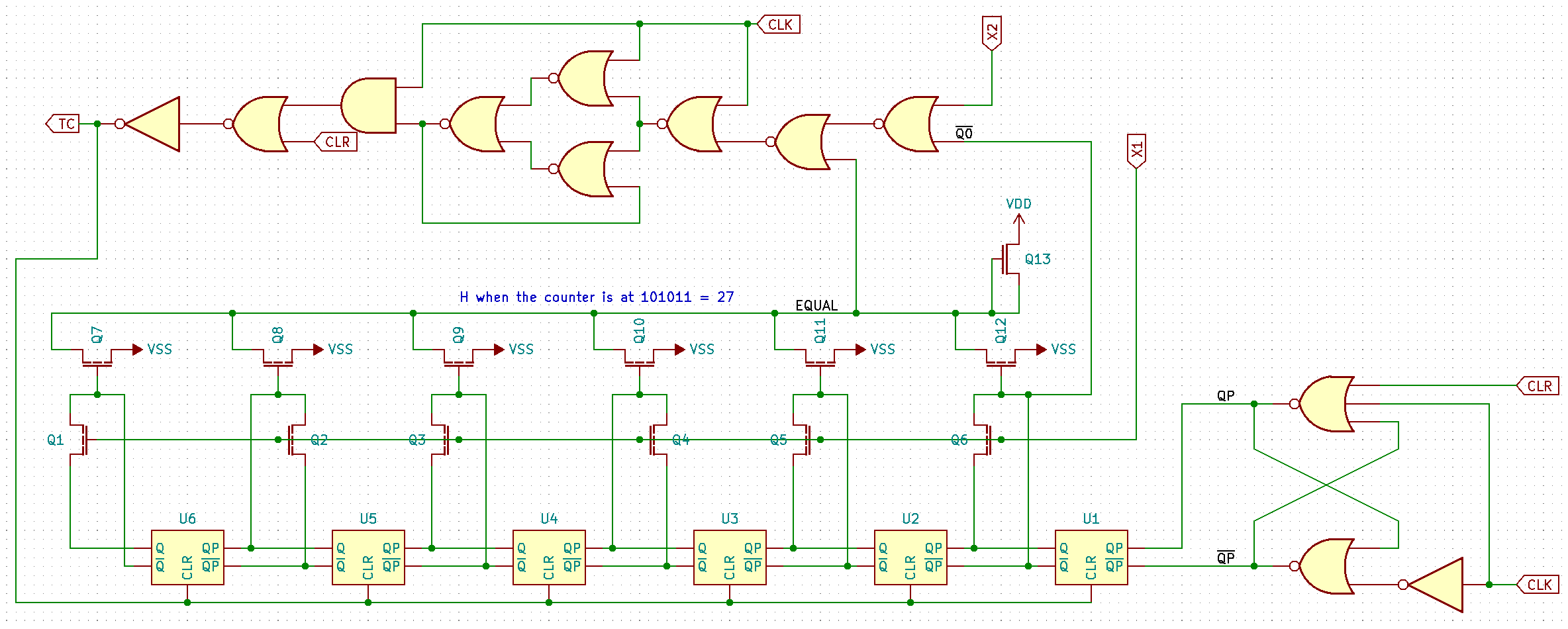
If anyone would be willing to simulate this for me to double check the work, I’d love to hear about that.
Worthy of note: there seems to be a bit of circuitry shoved into the yellow box is unaccounted for so far. For the moment, I do not have a clue what this is for; it does not appear to participate in the counter works at all. Oh, and it is not present / situated elsewhere in revision A2. Hmm…
Chain 2? 3?
This one took way too much time, really. I will tackle the other counters in the posts to come. Maybe tomorrow. Maybe next year.
Corrections? Comments? Get in touch, I’d love to chat about this.
XOXO, /DJ