Siemens M1327A3, part 6: TFF chain 3
Hola! I shall continue the reverse engineering exploits against Siemens M1327A3 today, and this time I will have a look at the final 3rd counter on the die.
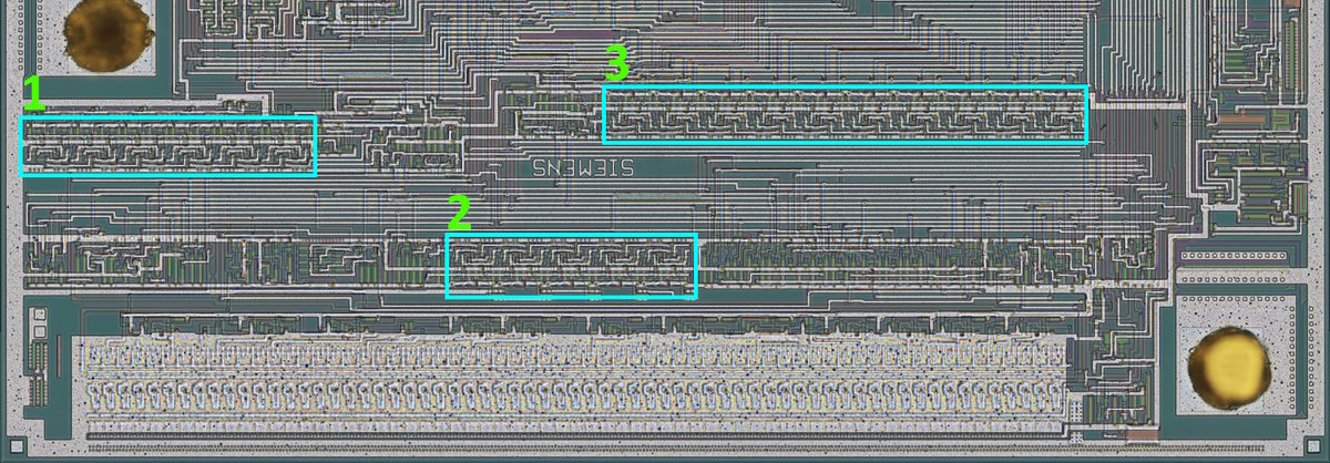
This chain has 10 T flip-flop (TFF) sections plus some more circuitry around them; one is directly above (red) and connected to the outputs and the other is to the right (yellow). Just like the other two.

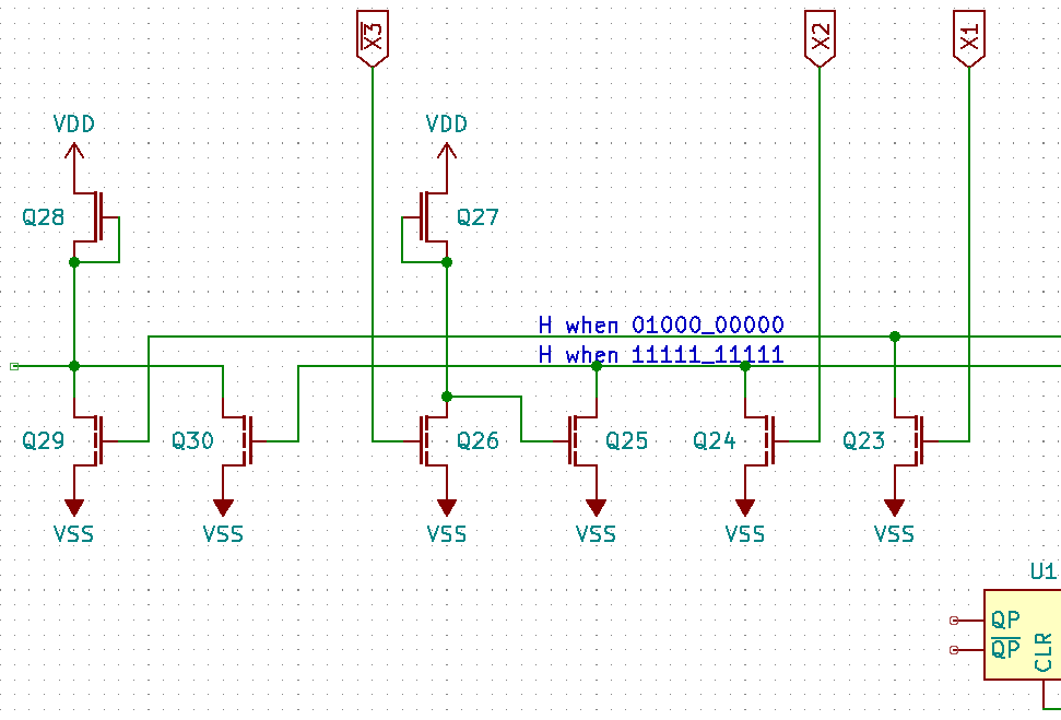
Let’s put the flip-flops and their output transistors on the schematic:

The transistors make up two NOR gates; the ones connected to the top line result in H when the count is 00000_00010 (MSB first), the bottom ones give H when the count is 11111_11111. Note that all outputs are also routed outside the unit.
Sketching out the rest of the red box circuitry…
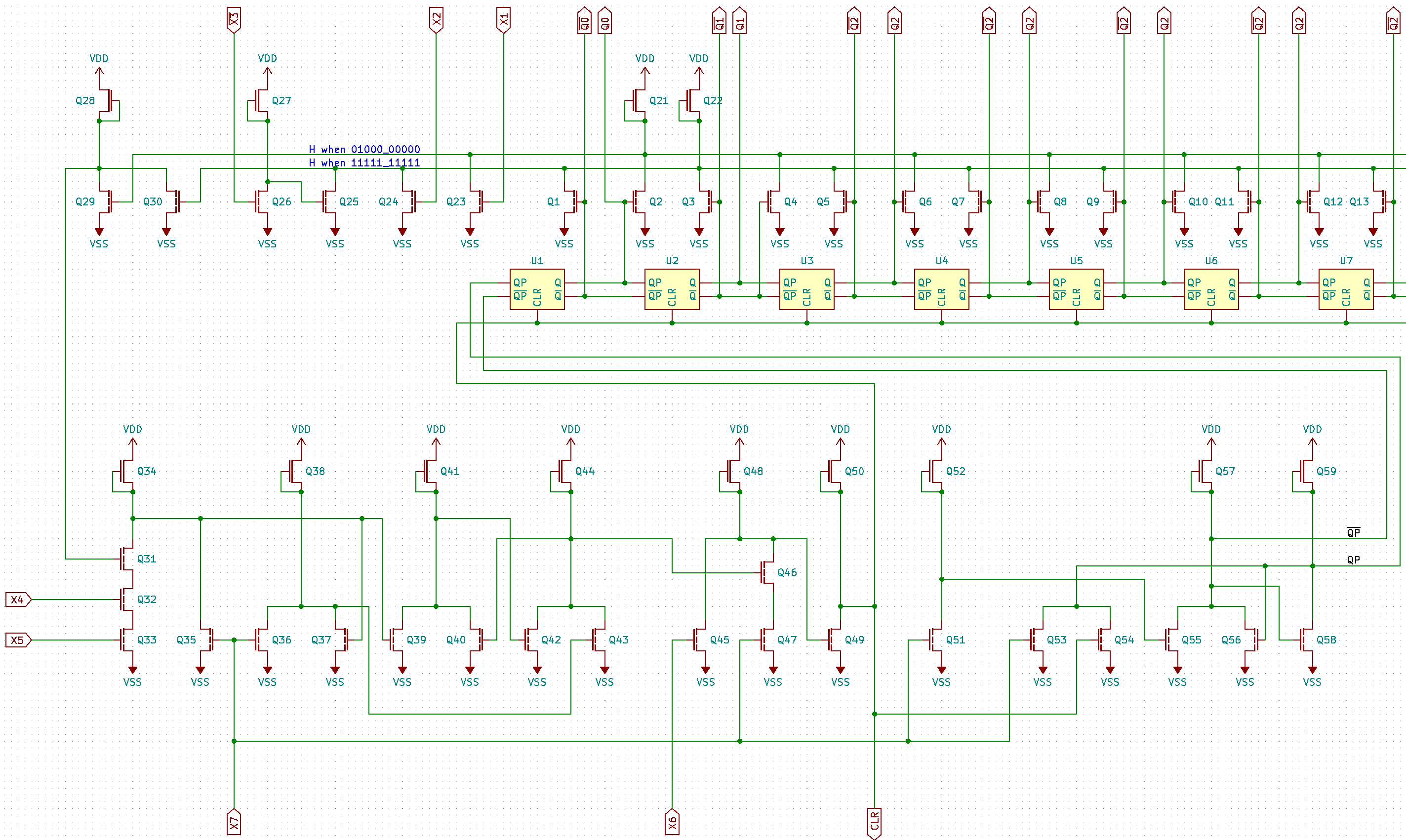
(A few hours later) I have drawn “the rest of the owl” = what was in the yellow box.
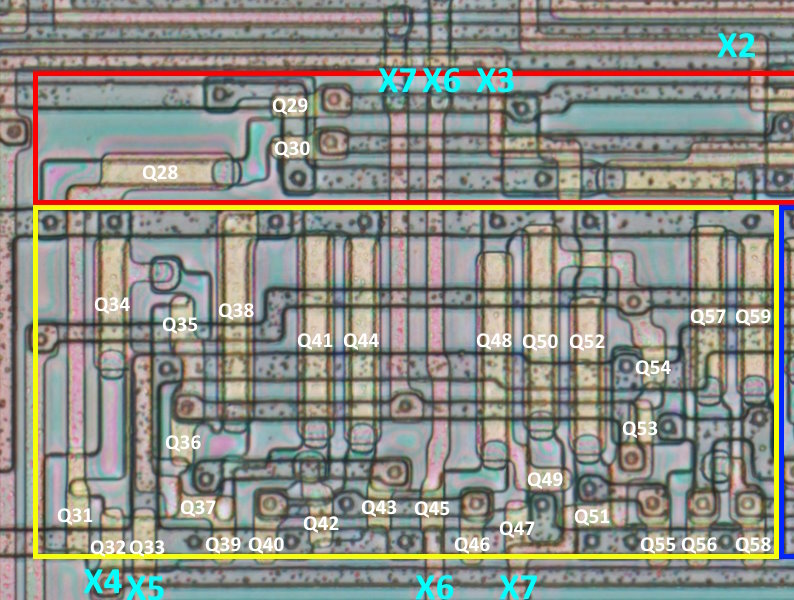
And a diagram of component/wire placement:
And after much moving and redrawing, here is the all-in-one schematic of this unit:
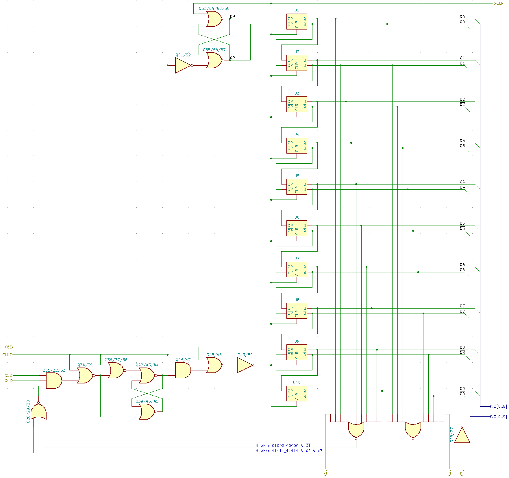
Yes, I discovered I can label the gates with transistors they are formed with. I should redo all the other unit schematics in this style…
Analysis
The clock generation stuff is already known circuitry. Thanks to that, I could mark X7 as CLK without investigating further. Same goes for CLR. But the way this signal is generated warrants further investigation.
X6 looks like an asynchronous clear input; will clear the flip-flop chain independent of anything. Otherwise, gate Q46/47 will synchronise the clear signal to the CLK high.
Gate Q28/29/30 outputs L when either of the signals generated with those massive NORs is H.
Y = !((CNT == 0b00000_00010 & !X1) + (CNT == 0b11111_11111 & !X2 & X3))

Y = !(CNT == 0b00000_00010 & !X1) & !(CNT == 0b11111_11111 & !X2 & X3)
The whole chain Q28 through Q33 outputs this:
Y = X5 & X4 & !(CNT == 0b00000_00010 & !X1) & !(CNT == 0b11111_11111 & !X2 & X3)

Y = !(!X5 + !X4 + (CNT == 0b00000_00010 & !X1) + (CNT == 0b11111_11111 & !X2 & X3))
The output is active low; it goes low when X5 or X4 is low or one of the counter values is matched (plus more condition inputs…). The rest of the circuit is identical to what’s seen in part 4, though this time I drew the flip-flop properly.
Now that chip deprocessing was successful, I can look further at what happens with this counter outputs. Let’s do that next time. Until then!
XOXO, /DJ
UPDATE, Aug 02: Counter values are now listed MSB first.