Siemens M1327A3, part 2: The funky shift register
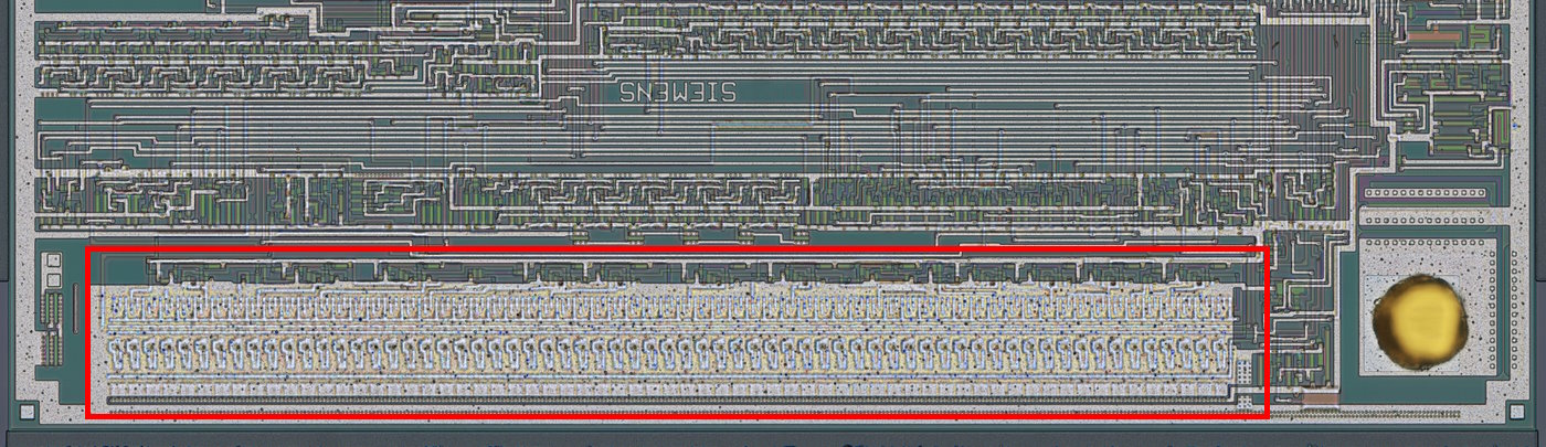
Hullo, today I shall continue the exploits against Siemens M1327A3. In this post, I will look at this fancy block, because why would anything boring be obscured with this much metal:
With metal (partially) removed, some detail emerges:
Again, all images are sourced from here for those playing along at home!
The repetitive structure continues throughout the whole length of the block, with some other circuitry is slapped here and there above it and connecting to some of exposed points.
For the lack of a better name right now, I will call this repetitive structure “the battery”. Maybe later on I’ll find a better name for it, but for now let’s roll with that.
Looking at the bigger picture, the whole block has only several connections to the rest of the chip:
- The top metal is connected to VSS
- On the very left, one wire goes into “the battery”
- On the very right, all the horizontal poly wires exit the block, one is connected to the VSS, others run off
- Again on the very right, a diffusion wire goes out to, eventually, the circuitry above the block of interest
- The logic above “the battery” only has two wires going out to the circuitry above the block of interest
This is great, it means it is something more or less self-contained and could possibly be understood in its entirety without the rest of the circuit.
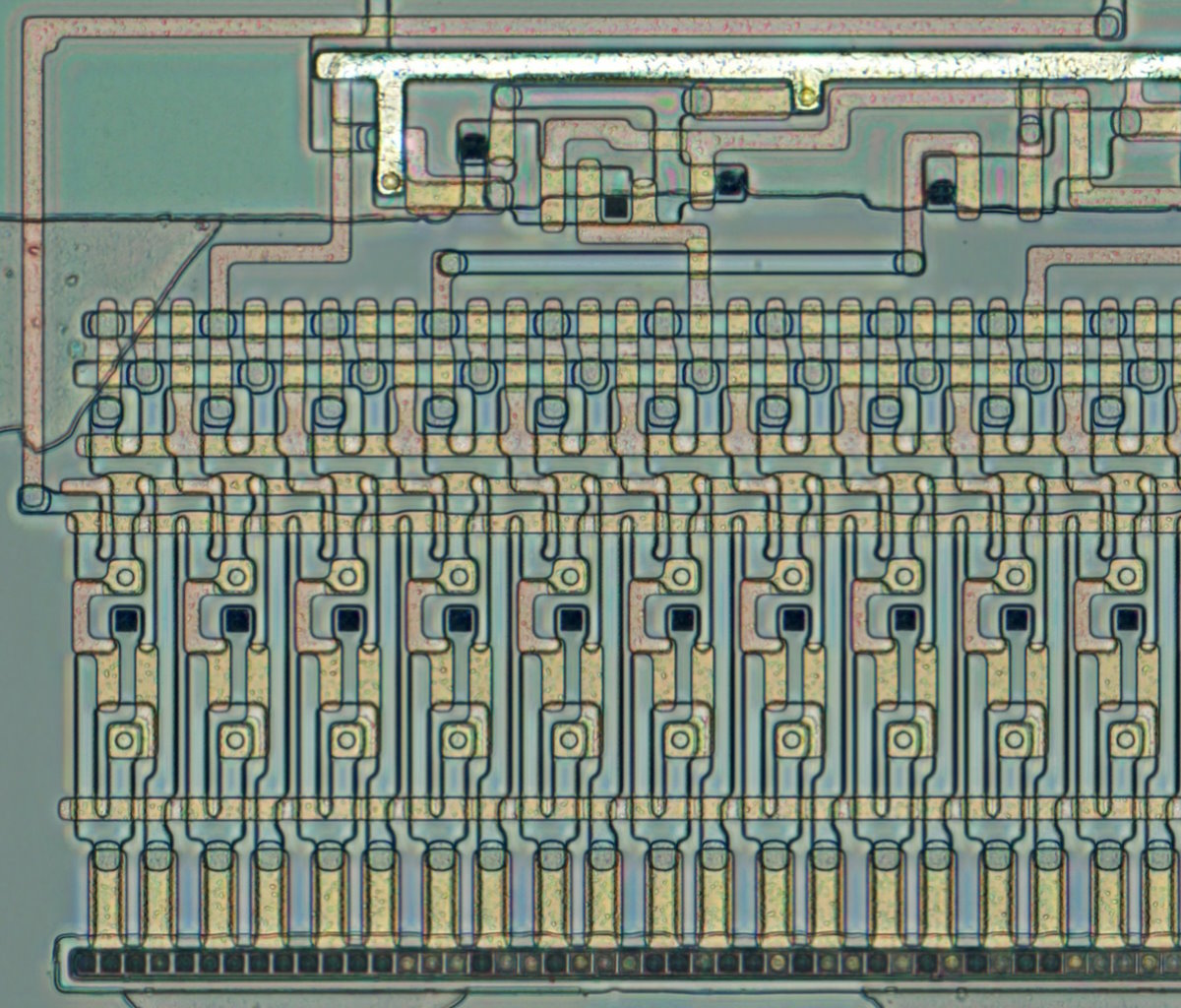
The battery
Visually, it would seem as if all the units in “the battery” are connected in series. A good assumption, but we’ll see if it holds.
Zooming in on the cells, there are 18 potential transistors in one unit:
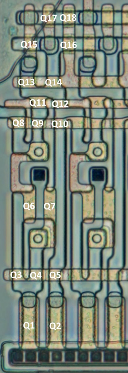
Redrawing this in KiCad close to the actual layout on the die:
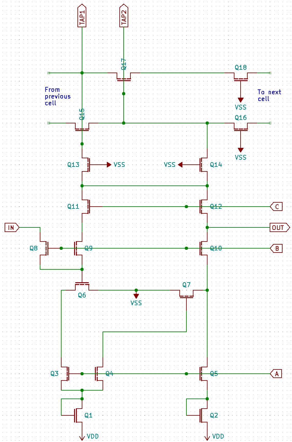
On this schematic:
INis where stuff presumably comes in, whether from the previous unit or from outside the blockOUTis where stuff presumably comes out; typicallyOUTis connected toINof the next cellA,B, andCare inputs – poly wires running horizontallyTAP1andTAP2are potential taps – going up to the circuitry to be explored later on
Now then, I say there is way too many transistors here; some of them are probably not actual transistors – see part 1. Have to weed them out. An “easy” way to do that is to spot the extra lines close to the channel; if they’re present – not a transistor! Saving you all the trouble, Q12, Q15, and Q17 can be discarded right away – all instances have them lines, thus none are actual poly gates. Looking closely, I can spot the lines to the left of Q3 and to the right of Q5; deleted. Same goes for Q9 and Q10. The schematic thus becomes this:
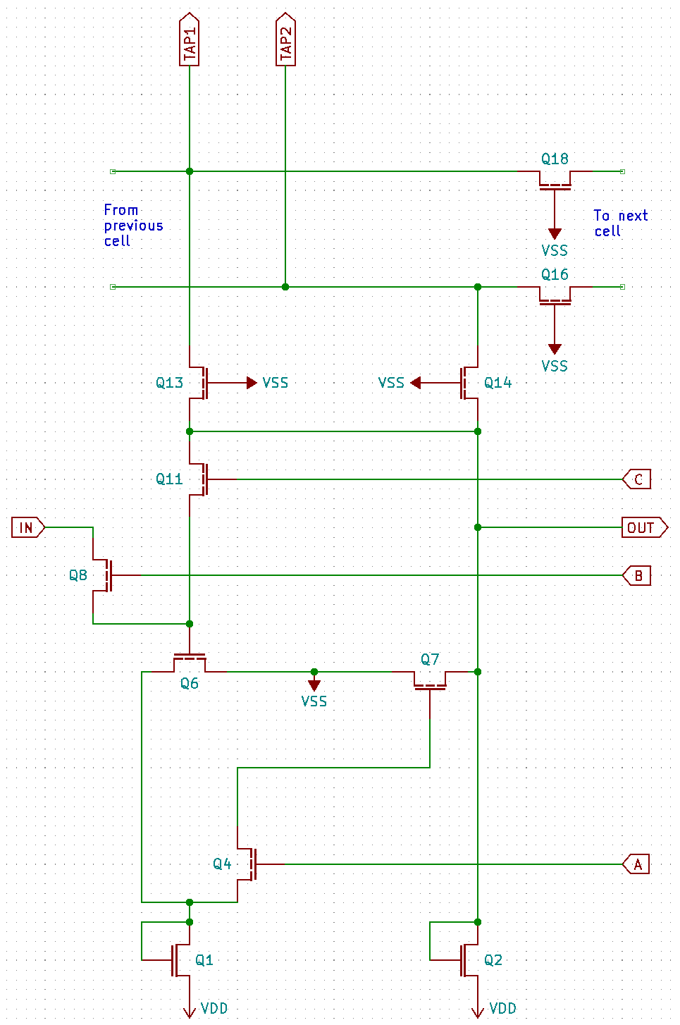
Much better! An astute reader will observe that Q1 and Q6 form an inverter, as do Q2 and Q7 – both are upside down here. The two inverters form a loop, if we temporarily disregard Q4 and Q11 – it’s a basic static memory cell! Then, Q4, Q8, and Q11 are pass transistors used to manipulate the cell state. To figure out how this operates, I’ll forget about Q13 and above for now.
Let’s say Q4 and Q11 are conducting, and Q6 is off; then Q7 is on and the cell output is L. Assume also that IN is at VDD. For it to propagate to the cell, Q8 must be conducting, and Q11 must be not – to avoid them fighting. Okay, assume that happens and Q8 is conducting now; then it pulls the gate of Q6 to VDD and it starts conducting, changing the inverter’s output state to L. But then, if Q4 is conducting, this state will propagate without limit through the whole chain – remember, the cells are chained together and ALL cells have Q8 conducting too. Thus Q4 must also be off before Q8 starts conducting. So for now, only the first inverter has changed state. Then, Q8 is turned off and Q4 is turned on, changing the state of the second inverter. Finally, Q11 is turned on, closing the loop and locking the cell state.
At least, this is what I think is going on.
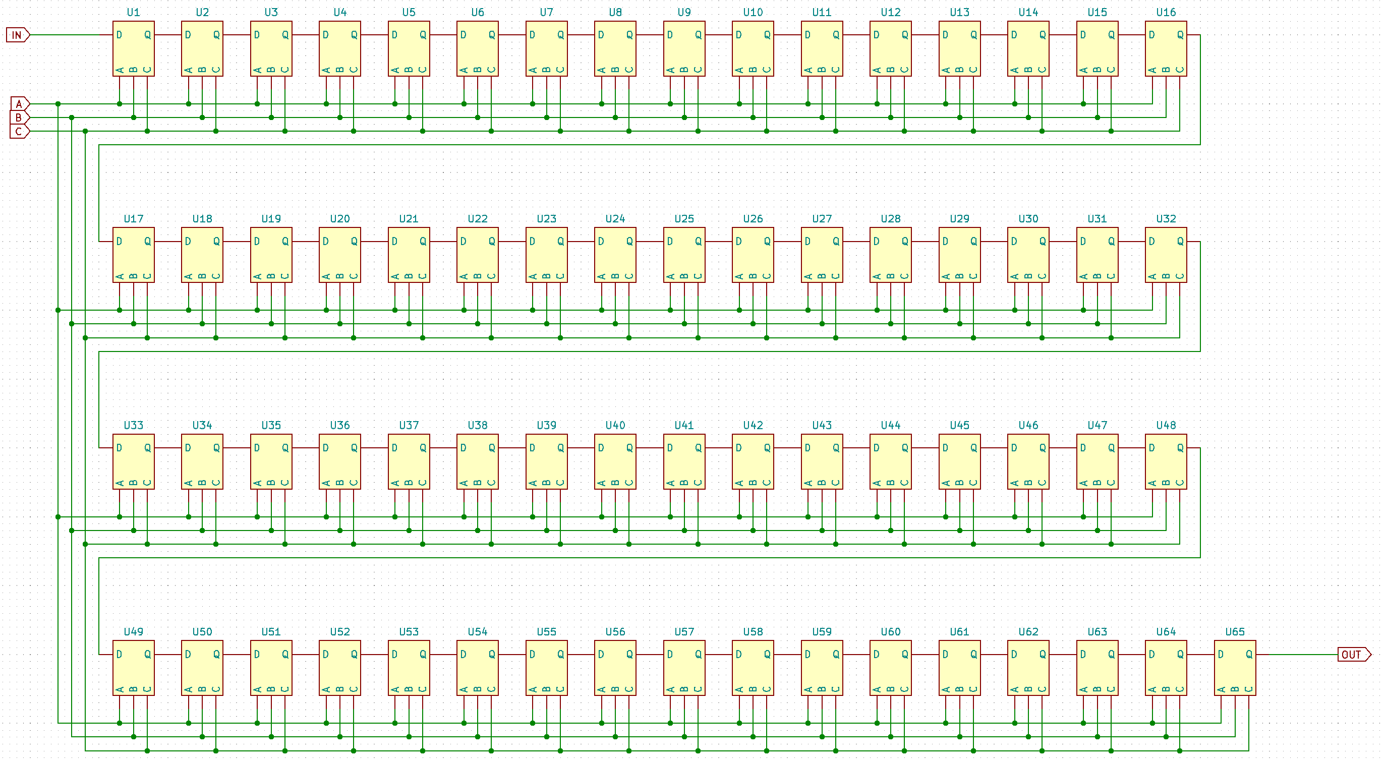
Repeating this process will shift data bits through the cells one by one. So, it’s a huge shift register! Counting the cells, there are 65 of them. Here is the schematic so far; input is D and output is Q, like on proper schematic.
But what about Q13 and friends?
Excellent question! Q13, Q14, Q16, and Q18 all have a common poly wire for their gates – and permanently connected to VSS. Any of these may be present or absent; absent transistors are just a wire and present transistors are open-circuit (their gate is connected to VSS so they never conduct assuming they are enhancement-mode). Considering the block as a whole, there are two horizontal diffusion “wires” running through it in the middle. Depending on whether Q13 or Q14 are present, cell output is connected to the lower or upper wire. Q16 and Q18, when present, isolate wire “segments” from each other. MENTAL, right? Why would anyone do that?! It’s so over-complicated. The only answer I could come up with was, this is done to obfuscate things: without deprocessing, an optical image won’t yield exact information on the taps, only approximate positions as poly wiring causing bulges on the metal layer so you can see that – but not which exact position it connects to. Notably, it is relatively easy to partially reconfigure the taps as the only mask to be edited is which of Q13, Q14, Q16, and Q18 are present.
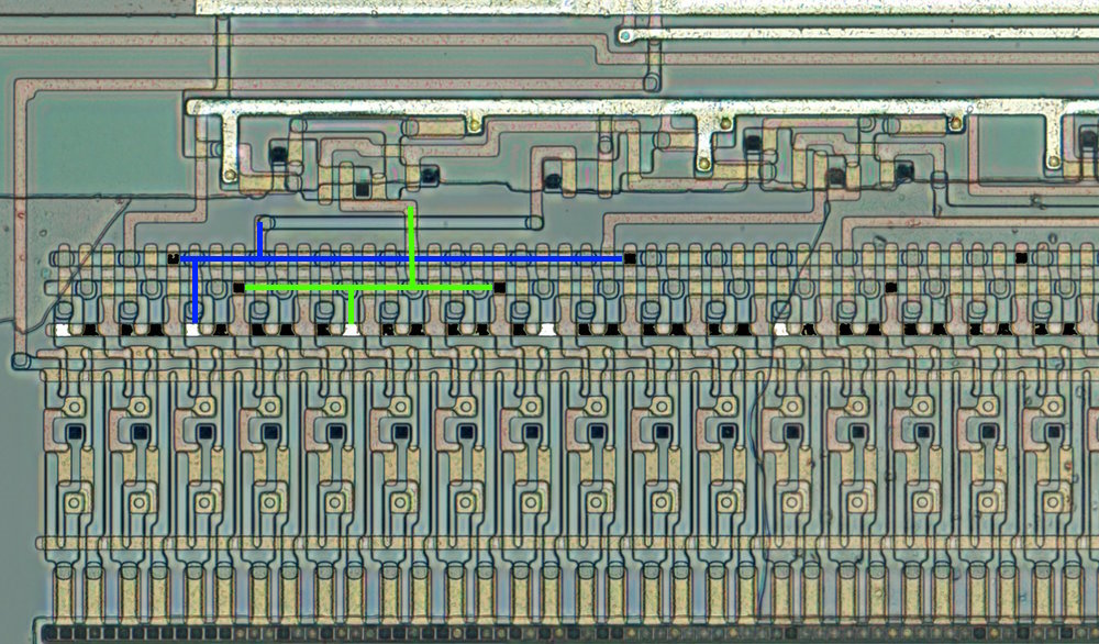
Going through all the cells and marking present/absent transistors (black = present = no connection), I see that indeed, only one cell is connected to each section of “wires”, without conflicts. I guess that counts as a confirmation of the theory above. These cell outputs are tapped off: 1, 3, 5, 8, 12, 18, 22, 25, 33, 37, 39, 44, 51, 54, 59, 61, 63, and 65.
Finally, the gates
Time to deal with the gates upstairs now. Well, in fact, one gate was already reverse engineered in part 1. There are several variations on the XOR theme, but in general they all follow the same schematic even though the layout differs for some reason.
The other kind of a gate in use here is a NAND. It’s so simple it makes no sense to conduct detailed RE here; just two NMOS transistors and a load stacked like a totem pole.
There are 16 gates in total there, and 2 outputs. Crunching through them and noting connections in KiCad, I got this schematic:
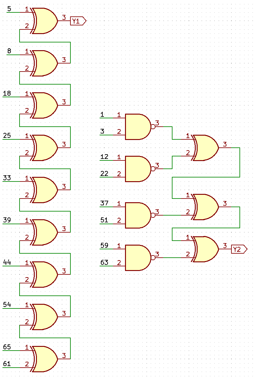
I wonder why we have two separate chains with absolutely different taps. I wonder why they decided to build this as a chain instead of a tree. I wonder why NAND gates are used. So many questions, and no answers (yet).
Well?
Beats me, honestly. I am not sure what this does exactly except that there is one long shift register and two combinatorial chains tapping it. Hope is to figure that out in future efforts. I am already happy with making this much sense of it.
Until then!
XOXO, /DJ